コンポーネントを選択するための6つのヒント 回路基板 design
The best 回路基板 設計方法:選択時に考慮すべき6つの事柄 回路基板 コンポーネント実装に基づくコンポーネント. この記事のすべての例は、マルチSIM設計環境を使用して開発されました, but the same concepts still apply even with different EDA tools.
1. Consider the choice of component packaging
In the entire schematic drawing stage, レイアウト段階で行う必要があるコンポーネントのパッケージとランドパターンの決定を考慮する必要があります. コンポーネントパッケージングに基づいてコンポーネントを選択するときに考慮するいくつかの提案を以下に与えます.
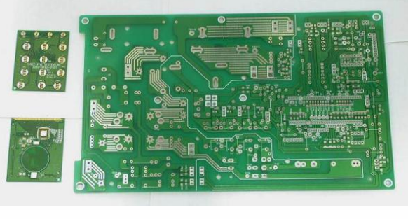
. 記憶する, the package includes the electrical pad connections and mechanical dimensions (X, Y, and Z) of the component, それで, コンポーネント本体とピンに接続するピンの形状 回路基板. コンポーネントの選択, あなたは、最終的なトップとボトム層に存在する可能性のあるインストールやパッケージの制限を考慮する必要があります 回路基板. Some コンポーネント (such as polar capacitors) may have high headroom restrictions, which need to be considered in the component selection process. At the beginning of the design, まず基本を描くことができます 回路基板 フレーム形状, and then place some large or position-critical components (such as connectors) that you plan to use. In この way, 仮想視点図 回路基板 (without wiring) can be seen intuitively and quickly, and the relative positioning and component height of the 回路基板 and components can be given relatively accurate. This will help ensure that the components can be properly placed in the outer packaging (plastic products, シャーシ, フレーム, etc.) after the 回路基板 is assembled. ツールメニューから3 Dプレビューモードを起動する 回路基板.

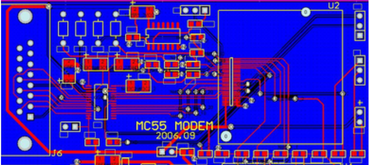
. The land pattern shows the actual land or via shape of the soldered device on the 回路基板. これらの銅パターン 回路基板 また、いくつかの基本的な形状情報が含まれます. The size of the land pattern needs to be correct to ensure correct soldering and the correct mechanical and thermal integrity of the connected components. When designing the 回路基板 レイアウト, you need to consider how the 回路基板 製造される, または手動ではんだ付けされるとパッドがはんだ付けされる方法. Reflow soldering (the flux is melted in a controlled high temperature furnace) can handle a wide range of surface mount devices (SMD). ウエーブはんだ付けは一般に使用される 回路基板 貫通穴を固定する, but it can also handle some surface mount components placed on the back of the 回路基板. 一般に, この技術を使うとき, the bottom surface mount devices must be arranged in a specific direction, そして、このはんだ付け方法に適応するために, the pads may need to be modified.
. コンポーネントの選択は、デザインプロセス全体で変更できます. Determining which devices should use plated through holes (PTH) and which should use surface mount technology (SMT) early in the design process will help the overall planning of the 回路基板. 考慮すべき要因はデバイスコストを含む, availability, デバイス面積密度, 消費電力, など. From a manufacturing perspective, 表面実装デバイスは一般にスルーホールデバイスより安価であり、一般により高い利用可能性を有する. 中小規模プロトタイププロジェクト, it is best to choose larger surface mount devices or through-hole devices, マニュアルはんだ付けを容易にする, しかし、エラーチェックとデバッグ中にパッドと信号のより良い接続を容易にする.
. データベースに既製パッケージがない場合, it is usually to create a customized package in the tool.
2. Use a good grounding method
Ensure that the design has sufficient bypass capacitors and ground planes. 集積回路を使用するとき, make sure to use a suitable decoupling capacitor near the power terminal to the ground (preferably a ground plane). コンデンサの適切な容量は、特定の用途に依存する, capacitor technology and operating frequency. When the bypass capacitor is placed between the power and ground ピンs and placed close to the correct IC pin, 回路の電磁両立性と感受性を最適化できる.
3. Allocate virtual component packages
Print a bill of materials (BOM) for checking virtual components. Virtual components have no associated packaging and will not be transferred to the layout stage. 材料の法案を作成し、デザインのすべての仮想コンポーネントを表示します. 唯一の項目は電源とグランド信号でなければなりません, 仮想コンポーネントと見なされるので, これは、概略環境でのみ処理され、レイアウト設計に送信されません. シミュレーション目的で使用されない限り, 仮想部品に表示されるコンポーネントは、カプセル化されたコンポーネント.
4. Make sure you have complete bill of materials data
Check whether there is sufficient data in the bill of materials report. After creating the bill of materials report, it is necessary to carefully check and complete the incomplete device, supplier or manufacturer information in all component entries.
5. Sort according to component label
To facilitate the sorting and viewing of the bill of materials, コンポーネント番号が連続して.
6. Check for redundant gate circuits
Generally speaking, すべての冗長ゲートの入力は入力端子をぶら下げるのを避けるために信号接続を有するべきである. すべての冗長または欠落したゲート回路を確認してください, そして、すべての有線の入力端子は完全に接続されています. 場合によっては, 入力端子が, システム全体が正しく動作できない. デザインでよく使われるデュアルオペアンプ. オペアンプの1つだけがデュアルオペアンプで使用されている場合 IC components, it is recommended to either use the other op amp, または未使用のオペアンプの入力を接地する, and deploy an appropriate unity gain (or other gain) ) Feedback network to ensure that the entire component can work normally.
In some cases, IC浮動ピン付きのSは仕様範囲内で正しく動作しないかもしれません. Usually only when the IC 同じデバイスのデバイスまたは他のゲートは、入力または出力がコンポーネントの電源レールの近くにあるか、または、飽和状態で働いていない, this IC それが働くとき、インデックス要件を満たすことができます. Simulation usually cannot capture this situation, シミュレーションモデルは一般的に IC together to model the floating connection effect