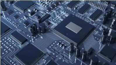
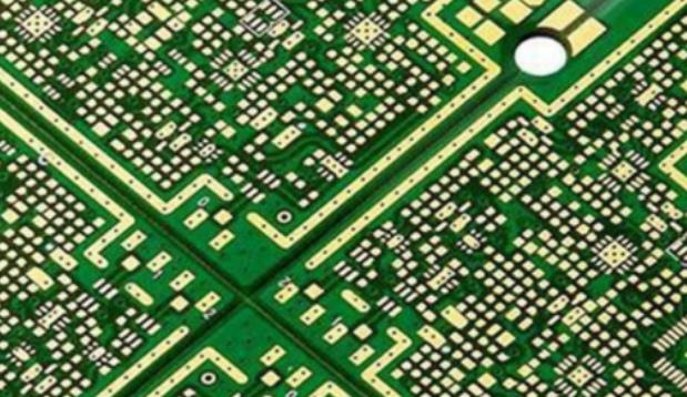
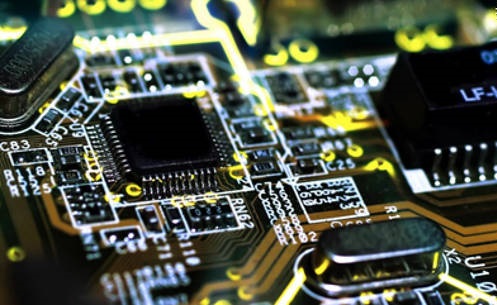
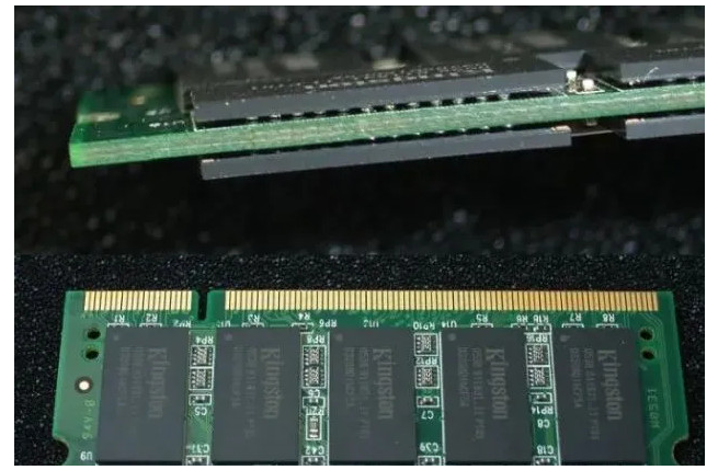
集成電路基板定義和功能
集成電路基板定義:用於封裝裸集成電路晶片的基板。
功能:
(1) Carrying semiconductor 集成電路 炸薯條.
(2) The internal circuit is arranged for the connection between the 炸薯條 and the circuit 板.
(3) Protect, 修理, 支持 集成電路 chip, 提供散熱通道, 是通信晶片和 印刷電路板.

集成電路封裝
出生:20世紀90年代中期,不到20歲。 新的集成電路(集成電路)高密度封裝形式,如BGA公司(球栅陣列封裝)和CSP(晶片尺寸封裝)的出現,為封裝帶來了一種必要的新載體——集成電路封裝基板。
* 電晶體 development: valve - Transistor - Through 洞 assembly - surface Packaging (SMT) - Chip level Packaging (CSP, BGA) - System Packaging (SIP)
* 印刷電路板 電晶體科技是相互依存的, 關, 穿透, 密切配合, 印刷電路板 可以實現多種晶片, 電力絕緣和電力連接之間的部件, 提供所需的電力特性.
技術參數層數,2~10層;
印刷電路板 板材厚度, 通常為0.1 ~ 1.5mm;
Minimum 印刷電路板 板 thickness tolerance *0 micron;
Minimum aperture, 通孔0.1毫米, 微孔0.03mm;
* Minimum pattern width/間距, 10~80 microns;
Minimum ring width, 50 microns;
* Contour tolerance, 0~50 micron;
* Buried blind hole, 阻抗, buried resistance capacity;
* Surface coating, 鎳/澳大利亞, 軟黃金, 硬黃金, 鎳/鈀/金, 等.
* Board size, â ¤150*50mm (single 集成電路 carrier);
That is to say, 這個 集成電路基板 需要更精細, 高密度, 高英尺數, 體積小, hole, 磁片, 線條更小, 超薄芯層. 因此, 有必要採用精確的層間對準科技, 模式成像科技, 電鍍工藝, 鑽井科技和表面處理科技. 對產品可靠性提出了更高的要求, 設備和儀器, 資料和生產管理. 因此, 科技門檻 集成電路基板 高,研發不容易.
與傳統科技相比的科技難點 印刷電路板 製造業, 需要克服的技術難題 集成電路基板 are as follows:
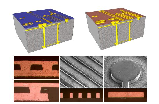
(1) core 板 production technology core 板 薄的, 易變形, 尤其是當板的厚度為0.2毫米, 帶板式結構, 板材膨脹和收縮, 層流參數, 層間定位系統等科技需要突破, 從而實現超薄芯板翹曲和壓制厚度的有效控制.
(2) Microporous technology
* Including: solder mask open process, 雷射打孔微盲孔工藝, 盲孔鍍銅填充工藝.
* Conformalmask (Conformalmask) process is used to make reasonable compensation for laser blind hole window opening, 通過打開的銅環直接定義盲孔的孔徑和位置.
* Indicators involved in laser drilling microhole: hole shape, 上下孔徑比, 側面侵蝕, 玻璃纖維突出, 孔底殘膠, 等.
* Indicators involved in blind hole copper plating include: filling capacity, 盲孔空腔, 下垂, 鍍銅可靠性, 等.
* At present, 微孔尺寸為50~100微米, 層狀孔隙數達到3個, 4和5訂單.
(3) Graphic formation and copper plating technology
Pattern compensation technology and control; Fine pattern production technology; Copper plating thickness uniformity control technology; Micro erosion control technology for fine pattern.
* The current pattern width spacing requirement is 20~50 microns. Copper plating thickness uniformity requirement is 18* micron, 蝕刻均勻性–90%.
(4) welding resistance process * including plug hole process, 焊接電阻印刷科技, 等.
* The height difference between the solder resistance surface of the 集成電路基板 小於10微米, 阻焊性與焊盤表面高度差小於15微米.
(5) Surface treatment technology
* Uniformity of thickness of 鎳/鍍金; 軟、硬鍍金工藝在同一板材上; 鎳/鈀/鍍金工藝.
* Lineable surface coating, 選擇性表面處理科技.
(6) Testing capability and product reliability testing technology
* Equipped with a number of testing equipment/與傳統樂器不同的樂器 印刷電路板 工廠.
* Master reliability testing techniques different from conventional ones.
(7) In general, 生產 集成電路基板 involving more than ten aspects of technology:
Graph dynamic compensation; Graphic electroplating process for thickness uniformity of copper plating; The whole process 材料 expansion and shrinkage control; Surface treatment process, 軟金和硬金選擇性電鍍, nickel/鈀/gold plating process;
* Core plate wafer production;
* High reliability detection technology; Microporous processing;
* If stacked micro 3, 4, 5, production process;
* Multiple laminated pressure; Laminate 4 times; Drilling 5 times; Electroplating 5 times.
* Wire pattern formation and etching;
* High precision alignment system;
* Welding stopper hole process, 電鍍填充微孔工藝;
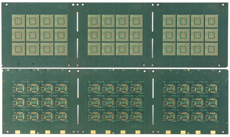
集成電路基板分類
通過封裝的形式

包裝趨勢
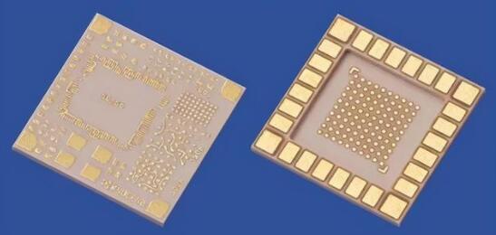
(1) BGA
*BallGridAiry, BGA, 球形陣列封裝.
* This kind of 包裹 of the 板 散熱,散熱, 電力性能良好, 晶片引脚可以大大新增, applied to 300 pin number (pincount) above 集成電路 package.
(2) CSP
*CSP, 晶片規模包裝, 晶片級尺寸封裝.
* Is a single 晶片封裝, 重量輕, 小的, 其包裝尺寸和 集成電路 本身大小幾乎相同或稍大, 用於記憶體產品, 通信產品, pin碼不高的電子產品.
(3) coated 水晶印刷電路板板
* FlipChip (FC) is a type of package in which the front side of the chip is flipped (Flip) and the convex block is directly connected 到 印刷電路板.
這種基板具有訊號干擾小的優點, 連接電路損耗低, 良好的電力效能, 高效散熱等.
(4) Multi-chip module
* Multi-chip (MCM) module Multiple chips with different functions in the same package.
* This is the best solution for electronic products to light, thin, 短的, 低於高速無線. 用於高階大型電腦或特殊效能電子產品.
* Because there are multiple chips in the same package, 訊號干擾, heat dissipation, 細線設計, 等等, 沒有更完整的解決方案, 屬於產品的積極開發.
按資料内容 s
(1) Hard 印刷電路板 board. 密封載荷 印刷電路板
* Rigid organic 包裝基板 made of epoxy, 英國電信, ABF樹脂. 其產值占 集成電路 packaging substrate. CTE (coefficient of thermal expansion) ranges from 13 to 17ppm/ 攝氏度.
(2)軟板密封加載印刷電路板板。
* The packaging substrate made of PI (polyimide), PE (polyester) resin flexible substrate, CTE為13~27ppm/ 攝氏度.
(3) Ceramic substrate
* Aluminum oxide, 氮化鋁, 碳化矽和其他陶瓷材料作為封裝基板. CTE較小, 6~8ppm/ 攝氏度.
以連接科技著稱
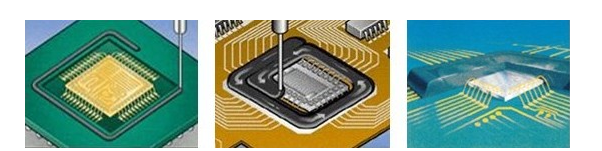
(1) Play pattern to engage the carrier plate
* The gold wire connects the 集成電路 to the 印刷電路板板。
(2) TAB 印刷電路板
*TAB -- TapeAutomatedBonding
* The inner pins of the chip are connected with the chip, 所述外引脚與所述包裝板連接.
(3)覆蓋晶體鍵合印刷電路板板。
*Filpchip, 晶圓經過Filp凸點,直接連接到 印刷電路板板。