The most reliable PCB & PCBA custom service factory.
Language

Language
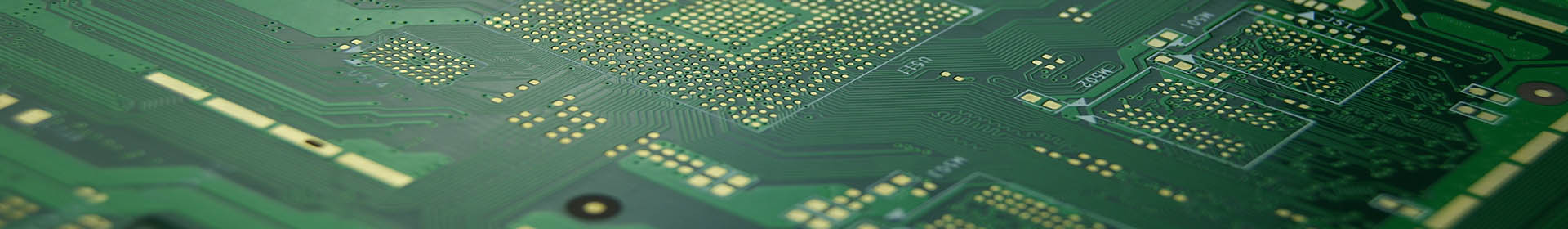
Board cuttign →UV Pattern→Etching→UV Soldermask→Silk screen→Outline→Surface Treatment→E-Test→Inspection
Single-sided PCB means that on the most basic PCB, the parts are concentrated on one side, the wires are concentrated on the other side, and the wires only appear on one side. Because single-sided PCB has many strict restrictions on the design of the circuit, because there is only one side, the wiring can not be crossed and must go around a separate path.
Single-sided PCB fabrication process and: single-sided copper clad laminate-blanking-photochemical method / screen printing image transfer-removal of resist printing-cleaning, drying-hole processing-contour processing-cleaning and drying-printed solder mask Coating-curing-printing marking symbols-curing-cleaning and drying-pre-applied flux-drying a finished product.
The single-sided PCB substrate materials are mainly paper phenol copper laminate and paper epoxy resin copper laminate. Single-sided circuit boards are mostly used in home appliances such as radios, heaters, refrigerators, washing machines, and commercial machines such as printers, vending machines, circuit machines, and electronic components. The advantage of single-sided printed PCBs is low price.
First of all, let's understand several concepts of PCB production:
(1) UNIT: UNIT refers to the unit graphics designed by PCB design engineers.
(2) SET: SET refers to a graphic that engineers put together a number of UNITs for reasons such as improving production efficiency and facilitating production. This is what we often call the puzzle, which includes unit graphics, process edges, and so on.
(3) PANEL: PANEL refers to a PCB formed by putting together multiple SETs and adding the tool board edge to improve efficiency and facilitate production when PCB manufacturers produce.
(4) Dry film: Dry film is the process of transferring the circuit pattern to the PCB board.
The concept of graphics transfer will be mentioned in PCB production, because the production of conductive graphics is the basis of PCB production. Therefore, the graphics transfer process is of great significance to PCB production.
The wet film process and manual lines in the PCB industry still occupy a very high market due to their cost factors. However, as many customers pay more attention to quality, wet film technology and manual lines will gradually be eliminated. ipcb company has already fully entered the era of automatic line dry film, and is the first PCB manufacturer to adopt fully automatic line dry film technology!
The process flow of PCB production is as follows
1. Cutting, filleting, edge planing
Cutting is the process of cutting the original copper clad laminate into PCBs that can be made on the production line, generally cutting into a work board of about 40*50cm.
2. Drilling
The effect of drilling the hole is shown in the figure. Because it is difficult to take a video of the inside of the hole with a camera, there is no copper in the hole at this time.
3, sink copper
After drilling in the previous step, there is no copper in the hole, that is, the via is blocked. At this time, the PCB board after drilling undergoes an oxidation-reduction reaction in the sinking copper cylinder to form a copper layer to metalize the hole. Copper is deposited on the surface of the original insulating substrate to achieve electrical inter-layer communication. !
4, laminating
A layer of blue dry film is pressed on the laminated PCB. The dry film is a carrier and is very important in the circuit process. The dry film process is also named for it. Compared with wet film, dry film has higher stability and better quality, and can be directly used as non-metalized vias.
5, exposure
Exposure: first align the circuit film with the PCB with the dry film pressed, and then place it on the exposure machine for exposure. The dry film is exposed to the energy of the lamp tube of the exposure machine, and the circuit film is placed where there is no circuit (where there is a circuit) Black, where there is no line is transparent) for full exposure.
After this step, the circuit is transferred to the dry film. The state at this time is that the dry film has a circuit that is not exposed, and the dry film has no circuit is exposed!
6, development
Development: Use the developer in the developing machine to develop the unexposed parts. The developer does not react to the exposed parts. So the final picture is yellow copper on the line part, and the part without the line is still blue (exposed dry film).
7, electric copper
Put the PCB into the electrical copper equipment, the part with copper is electrified with copper, and the part blocked by the dry film does not respond!
8, electric tin
Electric tin is to prepare the part of the copper that is protected by the dry film.
9, remove the film
That is, the blue dry film is returned. Because the circuit part already has tin, only a kind of stripping liquid is needed to react to the exposed dry film. Put it in the stripping machine, and the dry film will be easily removed.
10. Etching
After the unexposed dry film is removed by the developer, the copper surface will be exposed. The etching is to use a chemical solution (reacts to copper, but has no effect on tin) to corrode the unnecessary copper in the PCB, leaving the required part.
11. Withdrawal of tin
The tin stripping is to use a kind of potion (tin stripping water) to return the tin on the line, so that the line returns to its original color---copper.
12. Optical AOI line scanning
In the manufacturing process, defective products are inevitable due to various reasons such as man, machine, material, method, and environment. How can the quality of the line be guaranteed? There are generally two detection methods, one is to observe with the naked eye, and the second is the optical AOI used by ipcb. The working principle of AOI is to first use the high-definition image camera to quickly shoot, and then compare the captured pictures with the original files, which can fundamentally solve the hidden dangers of open, short, and slightly open, and short.
13. Printing solder mask oil
Print solder resist oil In this step, apply solder resist oil (including pads) to all areas of the PCB.
Solder mask, also called solder mask and green oil, is one of the most critical processes in the production of printed boards. It is mainly through screen printing or coating solder mask ink, and a layer of solder mask is applied to the board surface to prevent welding. Short circuit.
14. Solder mask exposure and development
The purpose is to remove the solder mask from the pads and other places. First put the solder mask film on the PCB covered with green oil, the film (the place where the window is to be opened is black, and the place where the window is not open is transparent), and then put it on the exposure machine for exposure, the part that is to be opened , Because the film is black, the black blocks the light and is not exposed. Now the state of the solder mask green oil has changed, part of the green oil is exposed, and the other part is the green oil that has not been exposed. From the surface, it is still green.
15. Characters (baking plate)
Print the position number of the device, the PCB board name and other characters on the PCB.
16. Surface treatment
But long-term exposure to the air is prone to moisture oxidation, and tends to exist in the form of oxides, and it is unlikely to remain as original copper for a long time. Therefore, surface treatment on the copper surface is required. The most basic purpose of surface treatment is to ensure good solderability or electrical properties.
Common surface treatments: spray tin, immersion gold, OSP, immersion tin, immersion silver, nickel palladium gold, electro-hard gold, electro-gold fingers, etc. (Jia Li create spray tin, immersion gold surface treatment).
17, forming the gong
Refers to turning the big board into a small PCB board, and the corresponding shape treatment.
18. Electrical test
Use needle test or general electromechanical performance to check whether there is an open or short circuit.
19. FQC This is the final quality control position, relying on people to control quality and quantity.
20, final inspection, random testing, packaging
Check the appearance, size, hole diameter, thickness, marking, etc. of the PCB to meet customer requirements. The qualified products are packed into bundles, which are easy to store and transport.


