
PCB design is based on the functions required by the customer. PCB design engineers design PCB schematics to achieve the tasks required by customers. The main work of PCB design is PCB schematic design, which needs to consider the layout of external connections and the shape and structure of the product. In addition, PCB board design needs to consider the optimum form of electronic components inside PCB, the optimum layout of circuit connections and PCB via holes, the factors of electromagnetic protection and heat dissipation. Excellent printed circuit board design can save PCB manufacturing costs and improve the performance of electronic products.
PCB design service is one of the ways for ipcb to help customers enter the market faster because iPCB company's PCB board design engineering team has rich practical experience in designing PCB to improve performance and manufacturability. IPCB focuses on PCB design of network communication, industrial control, medical treatment, aerospace; IC ATE test, computer, server, automotive electronics, equipment, and mobile phone.
What is PCB design?
1. If you are just an idea or concept or have already completed the schematic, we can convert it into a design document and then PCB manufacturing, PCB assembly, and testing. With more than 15 years of experience in the manufacture and body of the printed circuit board, we can ensure that the design fully meets the manufacturing requirements.
2. IPCB's PCB design team will work with you throughout the product development process to ensure that all design aspects are technically reviewed before the first production.
3. Once the PCB design is signed off for production, iPCB's highly skilled production team is on standby to build quality PCBA prototypes for initial test and development purposes.
4. With both machine and hand placement, parts can be populated to PCBs in as little as 48 hours, with full inspection as standard and additional tests on request.
5. iPCB aims to make the process as seamless as possible by offering all these services under one roof, saving you valuable time to focus on delivering your product to market.

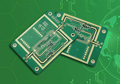
PCB design
iPCB's PCB design - A perfect "layout" electronic art for you
Based on PCB design and PCB prototype fabrication services, actively build PCB design, PCB manufacturing, SMT chip, material one-stop PCB Assembly business.
Senior PCB design and PCB layout team
More than 15 years of professional design experience, from PCB design to PCBA manufacturing to provide solutions. The best PCB design is "design quality" + "cost control" + "debugging convenience".
High difficulty PCB design experience
Good at high-frequency PCB, high-speed PCB, high-density PCB, mixed digital and analog, high power, high current, RF PCB, ate PCB, Rigid-Flex PCB, a high-speed backplane, etc. 2000 + PCB design experience every year.
Rich technical resources
Chip companies cooperate early, accumulate forward-looking technology, synchronize cutting-edge technology, master the most advanced technical information, and fully consider EMI, EMC, and manufacturability design.
High-quality management system
Standardized design management system, strict inspection, level by level, do not let go of any mistakes and details, to ensure that the failure rate is zero, 10000 + customers account monument accumulation.
High standard security measures
High standard confidentiality measures, signed a confidentiality agreement, the company's designer computer fully encrypted, the export of documents need to be fully approved, to ensure that the documents are 100% confidential.
Quality: perfect "design guide" and "design specification" provide additional technical suggestions beyond PCB layout, first-class training system, and training platform.
Self-inspection: self-inspection layout, wiring, rules, aesthetics, thermal design structure, etc
Review: ipcb senior team participate in the study together, from the schematic design, DFM, DFT, high speed, EMC, thermal design, and other comprehensive checks and mutual inspection
Mutual inspection: the best way to avoid personal thinking set, brainstorm, standardized and strictly controlled joint inspection system, perfect DFM review process
|
|
PCB Design Parameter Highest layers 42L Minimum line width 2.4mil Maximum number of pins 110000+ maximum connection 78000+ Minimum BGA pins spacing 0.3mm Maximum number of BGA-pins 2912 Highest speed signal 60GHZ Minimum line spacing 2.4mi |
PCB Design delivery date PIN Design delivery date Within 1000 3-5 days 2000-3000 5-7 days 4000-5000 8-12 days 6000-7000 12-15 days 8000-9000 15-18 days 10000-13000 18-20 days 14000-15000 20-22 days 16000-20000 22-30 days |
PCB design software
1. Protel, PROTEL 99SE, PROTEL DXP, and Altium are primarily used in China. These are software developed and upgraded by a company; The current version is Altium designer 15, which is relatively random and straightforward in design, but it is not very good to make complex PCB software.
2. Cadence SPB software cadence SPB this is cadence's software, and the current version is cadence SPB 16.5; OrCAD schematic design is an international standard; PCB design and simulation are complete, which is more complex than Protel, mainly due to complex requirements and settings; However, it has made provisions for the design, so the design gets twice the result with half the effort, which is more potent than Protel.
3. Bordstationg and ee of mentor company, among which, since word station is only applicable to a UNIX system, it is not designed for PC, so few people use it; The current version of mentor EE is mentor EE 7.9 and cadence SPB, which belong to the same level of PCB design software. It is worse than cadence SPB in some places. Its strengths are stay wire and flying wire, which is called the king of flying wire.
4. Eagle PCB design for easy layout is the most widely used PCB design software in Europe. The above-mentioned PCB design software is widely used. Cadence SPB and mentor are well-deserved kings. If you are a beginner in PCB design, I think cadence SPB is better. It can give designers a good design habit and ensure good design quality.
How to design PCB board? Four Stages of PCB Design
1. Refine the concept.--We summarize the objectives of the project and create a document to specify the project's technical scope.
2. Feasibility Study.--We conduct a study to examine whether the project will be possible within the client's budget. Agreed terms of reference will be set out. A draft report is presented to the client for feedback.
3. Hardware and Software Design.--We design the electronic circuit and produce the schematic designs, manufacturing bench-top prototypes. Software code is drafted.
4. Test and trials.--When software and hardware designs are complete we can begin serious bench testing. We continue until the design meets the project specifications.
Pre-preparation
Includes preparation of component libraries and schematics. Before PCB design, the schematic SCH component library and PCB component packaging library should be prepared first.
The PCB component package library is best built by the engineer according to the standard size data of the selected device. In principle, the component packaging library of PC is first established, and then the schematic SCH component library is established.
The requirement of a PCB component packaging library is high, which directly affects the installation of PCB. Schematic SCH component library requirements are relatively loose but pay attention to the definition of pin properties and the corresponding relationship with the PCB component packaging library.
PCB structure design
According to the size of the circuit board and the mechanical positioning, draw the PCB frame in the PCB board design environment, and place the required connectors, buttons/switches, screw holes, assembly holes, etc. According to the positioning requirements. Fully consider and determine the wiring area and the non-wiring area (how much area around the screw hole is the non-wiring area)
PCB design
Make the PCB schematic diagram according to the required product functions, draw the schematic diagram with the PCB schematic design tool, and generate the corresponding network table. Of course, in some special cases, such as when the circuit board is relatively simple and there is a network table, you can directly enter the PCB design system without schematic design. In the PCB design system, you can directly take part in packaging and manually generate the network table.
You can also manually change the network table to define the pads, not on the PCB schematic diagram such as the fixed pins of some components to the network connected to it, and those without any physical connection can be defined to the ground or protected ground, etc. Change the pin names of some devices with inconsistent pin names in the schematic diagram and PCB packaging library to be consistent with those in the PCB packaging library, especially diodes and triodes.
PCB layout
In PCB, there are some key components, core components, easily disturbed components, components with high voltage, components with high calorific value, and some heterosexual components. The location of these special components needs to be carefully analyzed. The layout with PCB meets the requirements of circuit function and PCB manufacturing and PCBA manufacturing. Improper placement of these components may cause circuit compatibility problems or signal integrity problems, resulting in the failure of PCB design.
When how to place special components in PCB design, first consider the PCB size. Ipcb believes that when the PCB size is too large, the printing line is long, the impedance increases, the dryness resistance decreases, and the cost increases; If it is too small, the heat dissipation is not good, and the adjacent lines are easy to be disturbed. After determining the size of PCB, determine the square position of special components. Finally, the PCB layout of all components of the circuit is carried out according to the functional units.
Fabrication PCB sample - PCB Assembly - PCBA board
This is a process from PCB samples to PCB design functions. This process needs a professional manufacturing team to complete. For example, some mistakes in the process will also lead to the failure of product development, so this is a very important process.
Procurement of components, replacement of compatible functional components, design of signal source, test rack, etc.
We promise to provide you with convenient and fast service at any time with high-quality product quality, low price, perfect and timely technical support, and we sincerely welcome you to consult and negotiate business.
PCB design mainly involves product categories
Network equipment, Bluetooth equipment, C, Ku band tuner, large router, digital camera, digital video recorder, other high-precision electronic products, laptop motherboard, DVB, satellite receiver, wireless communication module, PCB motherboard, mobile phone, PHS, walkie talkie, DVD, portable visual equipment
PCB design service advantages
1. Strong backing, senior expert
IPCB company's senior experts provide technical guidance and support to provide the most powerful guarantee for your PCB design quality.
2. Strict process and standardized guarantee
The strict design process, meticulous R & D team, perfect design specifications, and classic cases minimize your PCB design risk.
3. Close service and large-scale team
The software and hardware engineers who have been engaged in technical development and PCB design for many years entirely create the best communication and a strong PCB design team to meet the sudden needs of customers in any case
4. Own software to improve efficiency
A unique platform group is established to develop tool software in line with their characteristics for the existing platform, which significantly improves work efficiency and shortens the PCB design cycle.
5. Keep up with the frontier and keep pace with the times
Pay close attention to the latest developments in the industry, keep up with the cutting-edge technology of the industry, and communicate closely with the advanced technology of the industry to ensure the best guarantee of high-end PCB design

PCB design process
In electronic design and development, attention should be paid to PCB design and electronic component selection.
1. PCB design shall consider wiring, SMT difficulty, separation of analog circuit and digital circuit, electromagnetic interference between components and circuits and other related issues. Pay special attention to the problem of interference, because such problems are sometimes hidden problems, which may appear at some time. It would be embarrassing if it appeared after large-scale production.
2. For the problem of component selection, the use of side door should be avoided in the selection of electronic components, because this component may face shutdown at any time or be difficult to be compatible with other components. Sometimes replacing a component will cause great trouble because the pin pin pin or drive is incompatible. For products, the use of mature and stable components can not only improve the stability of products, but also sometimes reduce the cost of products.
After the PCB board is designed, the PCB sample can be carried out. After the PCB sample is completed, the firmware can be burned to test and optimize PCBA.
IPCB company's PCBA design technology advantages include manufacturability (DFM), testability (DFT), and design for assembly (DFA)
High Density, B/B PCB design
Thermal consideration in PCB design
Design process optimize
New design methodology or technology
PCB stack-up optimal design
Signal Integrity simulation & analysis
EMC in board design
Power Integrity analysis
SI application in practical product design
PCBA design technique for a particular product
Design skill dealing with Power signals
Teamwork in PCB design
EDA software advanced function & application
Introduce new layout & Simulation
IC package design technique
Design for Cost-down consideration
IPCB is a professional PCB and PCBA manufacturing company. We provide RD and production products from PCB design to PCB manufacturing, PCB assembly to completion. If you have a good idea, please contact IPCB.


