
Printed circuit boards have been developed for more than 100 years. The design of PCB board is mainly electronic board layout design. The main advantage of using printed wiring board is to greatly reduce errors in wire layout and electronic product assembly, and improve the level and production efficiency of automatic manufacturing of electronic products.
Before the appearance of printed circuit board, the interconnection between electronic components depended on the direct connection of wires to form a complete circuit. In contemporary times, the circuit board exists only as an effective experimental tool, and it has become an absolutely dominant position in the electronic industry. At the beginning of the 20th century, in order to simplify the production of electronic machines, reduce the wiring between electronic parts, and reduce the production cost, people began to study the method of replacing wiring by printing. Over the past three decades, electronic engineers have proposed to use metal conductors as wiring on insulated substrates. The most successful was in 1925, when Charles Ducas of the United States printed circuit patterns on insulated substrates, and then successfully established conductors for wiring by electroplating.
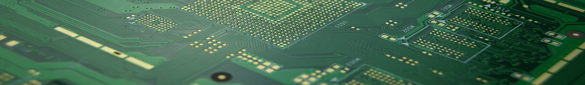
It is a non-conductive material printed or etched with conductive leads. Electronic components are installed on the circuit board, and each component is connected by leads to assemble or form a working circuit. The circuit board can have one or two layers of conductors, or multiple layers of conductors and multiple conductive interlayers, each separated by an insulating layer. The most commonly used circuit boards are made of plastic or glass fiber, resin composites, and copper wires. Of course, other materials are also used. Most pcb boards are flexible board or rigid circuit board, and flexible layers can also be used in curved spaces. Components can be installed using SMD or via technology.

manufacturers
If the manufacturers are defined according to their capacity, they currently account for more than 80% of the world's PCB capacity. Although the pcb industry as a whole is not very different, each manufacturer has its own expertise. The watershed of its technical level lies in its electroplating and etching. At present, the capacity of iPCB company is 3mil/3 mil for standard FR-4 pcb plate and 1.5mil/1.5mil for HDI pcb substrate. The line width/spacing of IC substrate is 30um/30um. iPCB also has a deep understanding of microwave high frequency PCB. iPCB is a good manufacturer in China.
What is printed circuit board assembly?
It is a product of the bare circuit board with electronic components installed. The electronic devices on pcb boards can be SMT electronic devices, DIP electronic devices, and assemblies. For example, the server motherboard is a process of making assemblies of it.
How to test a pcb plate when its assembly is completed? This is also known as the ICT test, which requires an assembly station to install button batteries, radiators, CPU base brackets, CPU backplates, handles, some isolation mylar, Limited plastic columns, screws, etc. A server motherboard with assemblies is composed.
PCB assemblies require some external force to be applied to the printed wiring board assemblies, so the assemblies need to be fixed and supported on the assembled fixtures before they are assembled. Some pcb assemblies need to be assembled on the soleplate,so two supporting fixtures need to be made. Support fixtures also need to pass electrostatic protection and stress tests before they are delivered to the production line for use. The standard of electrostatic protection can be referred to as ANSI/ESD S20. The stress test is referred to IPC-JEDEC-9704A(L).
The plastic combs we use in our life are very easy to generate static electricity, especially when the winter is very dry, the hair will fly up. When we have static electricity on our body and just touch the metal door handle, our hands will feel an electric shock. Similarly, static electricity can also be harmful to electrostatic sensitive devices such as IC on printed wiring board assembly, and the test of the process may not be completely screened out. You can use a finger sleeve to avoid discharging and dirt when you handle the battery. In addition, the battery is polar, you need to pay attention to checking the positive and negative poles of the battery during installation.
Consists mainly of the following components
1. Pattern: Circuits are used as a means of conducting between originals. Large copper faces are designed as grounding and power layers in the circuit board. The circuit and the surface are made at the same time.
2. Dielectric layers: They are used to maintain the insulation between the circuit and layers, so they are called circuit substrates.
3. Through hole/ via Through-hole allows circuits above the double sided pcb to connect to each other, larger through holes are used as part plug-ins, and nPTH is usually used for surface mounting positioning and for fixing screws when assembling.
4. Solder-resistant/Solder Mask: Not all copper surfaces need tin parts, so in areas that are not tin-eating, a layer of material (usually epoxy resin) will be printed to prevent short-circuiting between non-tin-eating routes. They are divided into green oils according to different processes. Red oil. Blue oil.
5. Legend/Marking/Silkscreen: This is an unnecessary component. The main function is to label the names of parts on the printed circuit board. Position box for its repairs and identification after pcb assembly.

Design
We can use free printed wiring board software for circuit board design. The ultimate goal of our circuit board design is to design a correct, reliable, and beautiful PCB.
Before drawing, all aspects must be well prepared. If the schematic diagram is drawn correctly, enter the appropriate pin encapsulation for each schematic element according to the actual element. Plan the shape and size of the printed wiring boards according to the size or design requirements of the electrical enclosure. The type of it is determined according to the density of circuit board components and the complexity of wiring. Measuring circuit has positioning requirements for the positioning dimensions of components, such as potentiometers, the distance of various sockets from the border of the circuit board, the size and positioning of the mounting holes, etc. For more specific components, if a suitable package cannot be found in the printed circuit board package library, the homemade component package must be designed, manufactured, and invoked.
After the plan, the component pin packaging and network can be loaded. Generally, various errors may be encountered when loading the component pin packaging and network. At this time, according to the error prompts, you should go back to the schematic diagram to modify, and then reload the component pin packaging and network until the error is eliminated. After loading the pin packages and networks of the components, the components can be automatically laid out and manually adjusted according to the layout principle to make the positions of the components conform to the product layout requirements and facilitate wiring.
After the component layout is completed, wiring can be done. Wiring generally combines automatic wiring with manual wiring. Before automatic wiring, automatic wiring rules must be set up to determine the wiring level, wire width, and other parameters to prepare for automatic wiring. In general, during the process of automatic wiring, the system lays emphasis on the traverse's distribution rate, which leads to the result that there must be some traverse lines that bend too much and are too long to meet the requirements of electrical characteristics. At this time, manual modification must be made. At the same time, according to the actual needs and the requirements of improving the anti-interference ability and reliability, copper cladding, installation holes, and teardrop filling can be added to the printed circuit board. Also, modify and add component labels, dimension labels, text labels, and so on.
After the design is completed, the design and fabrication can be sent to the manufacturer according to the number of produced.
Fabrication
iPCB has advanced printed circuit board equipment and sufficient manufacturing materials in stock, We provide standard custom services. If you have a conclusion about the printed circuit board, please contact iPCB.


