Language
Language
Calculation of characteristic pcb impedance
Simple characteristic pcb impedance model: Z=V/I, Z represents the impedance of each step in the signal transmission process, V represents the voltage when the signal enters the transmission line, I represents the current.I is plus or minus Q over plus or minus t, Q is the charge, and t is the time of each step.

Power (from battery) : ±Q=±C×V, C stands for capacitance, V stands for voltage. Capacitance can be derived from the unit length of the transmission line capacity CL and the signal transfer speed v.Unit value as a speed the length of the pins, then multiplied by the time needed for each step t, then get the formula: + C = CL * v * (+ / -) t. comprehensive above, we may safely draw the characteristic pcb impedance, Z = v/I = v/(+ Q / + t) = v/(x + C v / + t) = v/(CL * v/v * (+) t + t) = 1 / (CL (v)
It can be seen that the characteristic pcb impedance is related to the unit length capacity of transmission line and the signal transmission speed.In order to distinguish the characteristic impedance from the actual impedance Z, we add 0 after Z. The characteristic impedance of the transmission line is: Z0=1/(CL×v)
1. Impedance introduction
1. Definition of characteristic impedance: at a certain frequency, in the transmission signal line of an electronic device, relative to a certain reference layer, the resistance suffered by its high-frequency signal or electromagnetic wave during the propagation process is called characteristic impedance, which is electrical impedance , Inductive reactance, capacitive reactance... a vector summation.
2. Classification of characteristic impedance: single-ended (line) impedance, differential (dynamic) impedance, and coplanar impedance.
Single-ended (line) impedance: English Single Ended Impedance refers to the measured impedance of a single signal line.
Differential (dynamic) impedance: English Differential Impedance, refers to the impedance measured in two transmission lines of equal width and equal spacing during differential drive.
Coplanar Impedance: English Coplanar Impedance , refers to the impedance measured when the signal line is transmitted between GND/VCC around it (the distance between the signal line and GND/VCC on both sides is equal).
3. Conditions for impedance design: When a signal is transmitted in a PCB wire, if the length of the wire is close to 1/7 of the signal wavelength, the wire at this time becomes a signal transmission line. Generally, signal transmission lines need to be impedance controlled. When making PCB, decide whether to control the impedance according to the customer's requirements. If the customer requires impedance control for a certain line width, the impedance of the line width needs to be controlled during production.
4. When the signal is transmitted on the PCB, the characteristic impedance of the PCB must match the electronic impedance of the head and tail components. Once the impedance value exceeds the tolerance, the transmitted signal energy will be reflected, scattered, attenuated or delayed. , Resulting in incomplete signal and signal distortion.
5. Influencing factors of impedance:
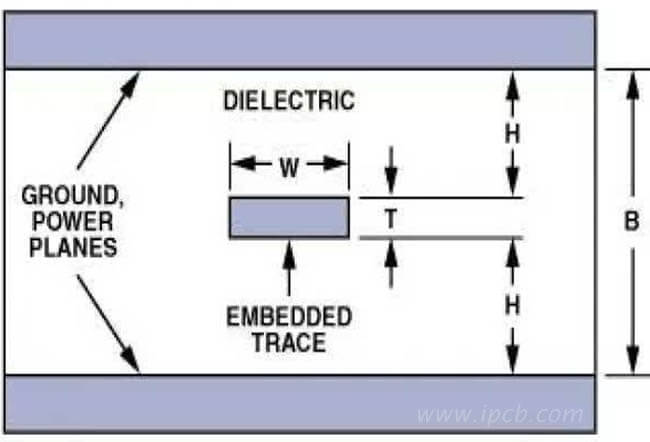
1), Er: The dielectric constant of the medium is inversely proportional to the impedance value. The dielectric constant is calculated according to the newly provided "Sheet Permittivity Table".
2), H1, H2, H3... The thickness of the dielectric between the circuit layer and the ground layer is proportional to the impedance value.
3) W1: the width of the bottom of the impedance line; W2: the width of the top of the impedance line, which is inversely proportional to the impedance.
A: When the inner bottom copper is 1oz, W1=W2+0.5mil; when the inner bottom copper is 2oz, W1=W2+1.2mil.
B: The bottom copper of the outer layer is 1oz, W1=W2+1.2mil; when the bottom copper of the outer layer is 2oz, W1=W2+1.6mil.
4) T: Copper thickness, which is inversely proportional to the impedance value.
A: The inner layer is the copper thickness of the substrate, Hoz is calculated as 15um; 1oz is calculated as 30um; 2oz is calculated as 65um.
B: The outer layer is the thickness of the copper foil + the thickness of the copper plating, depending on the hole copper specifications. When the bottom copper is Hoz, the hole copper (average 20um, the minimum 18um), the surface copper is calculated as 45um; the hole copper (average 25um, the minimum 20um), the table copper is calculated as 50um; when the minimum single point of hole copper is 25um, the table copper is calculated as 55um.
C: When the bottom copper is 1oz and the hole copper (average 20um, minimum 18um), the surface copper is calculated as 55um; when the hole copper (average 25um, minimum 20um), the surface copper is calculated as 60um; when the hole copper single point is minimum 25um, The table copper is calculated at 65um.
5) S: The distance between adjacent lines and lines is proportional to the pcb impedance value (differential impedance).
6), C1: the thickness of the base material solder mask, which is inversely proportional to the pcb impedance value;
C2: The thickness of the wire surface solder mask, which is inversely proportional to the pcb impedance value;
C3: The thickness of the solder mask between wires, which is inversely proportional to the impedance value;
CEr: The dielectric constant of the solder mask is inversely proportional to the impedance value.
A: Print solder mask ink once, C1 value is 30um, C2 value is 12um, C3 value is 30um.
B: Print solder mask ink twice, C1 value is 60um, C2 value is 25um, C3 value is 60um.
C: Cer (dielectric constant of solder mask): Calculated according to 3.4.