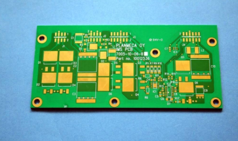
What matters should be paid attention to in the design of multi-layer PCB board?
Circuit boards can be divided into single-sided boards, double-layer boards and multi-layer boards according to the number of layers. Multi-layer boards refer to circuit boards with more than 4 layers. For many miniaturized products and high-speed products, multilayer boards are used, such as mobile phones, routers, and switches. So, what matters should be paid attention to in the design of multi-layer PCB board?
1. Why use multi-layer boards?
1. Requirements for product miniaturization:
At present, electronic products are moving closer to miniaturization, but there are not many chips and components used, so that PCBs cannot be routed, and the area can only be exchanged by the number of layers.
2. Requirements for high-speed signal integrity:
With the development of electronic technology, high-speed signal products such as routers, mobile phones, switches, and base stations are susceptible to interference and crosstalk. Multilayer boards can effectively improve signal integrity and minimize signal interference.

2. Matters needing attention:
1. Pay attention to the distribution of each layer, which is directly related to the performance of the product.
Take a 4-layer board as an example. Four-layer boards have multiple distribution methods: signal layer, power layer, GND layer, signal layer or power layer, signal layer, signal layer, GND layer; the general distribution principle is as follows: signal layer and GND layer are adjacent to shield interference The tight coupling between the power supply layer and the GND layer is conducive to the stability of the power supply, and the high-speed signal is loaded between the two copper-clad layers as much as possible to reduce interference.
2. Do you want a negative film method?
The so-called negative film method is that the entire plane is a piece of copper, and the copper is cut through one line, which is very different from the usual wiring. This negative film method is more commonly used in the power layer and GND layer.
In short, the design content of multi-layer boards is very much, and the above are just two things that need to be paid attention to when designing multi-layer PCB boards. iPCB is a high-tech manufacturing enterprise focusing on the development and production of high-precision PCBs. iPCB is happy to be your business partner. Our business goal is to become the most professional prototyping PCB manufacturer in the world. Mainly focus on microwave high frequency PCB, high frequency mixed pressure, ultra-high multi-layer IC testing, from 1+ to 6+ HDI, Anylayer HDI, IC Substrate, IC test board, rigid flexible PCB, ordinary multi-layer FR4 PCB, etc. Products are widely used in industry 4.0, communications, industrial control, digital, power, computers, automobiles, medical, aerospace, instrumentation, Internet of Things and other fields.