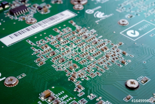
Electromagnetic compatibility refers to the ability of electronic equipment to work in a coordinated and effective manner in various electromagnetic environments. The purpose of electromagnetic compatibility design in PCB design is to enable electronic equipment to suppress various external interferences, to enable electronic equipment to work normally in a specific electromagnetic environment, and to reduce the electromagnetic interference of electronic equipment itself to other electronic equipment.
1. Choose a reasonable wire width
Since the impact interference generated by the transient current on the printed lines is mainly caused by the inductance of the printed wires, the inductance of the printed wires should be minimized. The inductance of the printed wire is proportional to its length and inversely proportional to its width, so short and precise wires are beneficial to suppress interference. The signal lines of clock leads, row drivers or bus drivers often carry large transient currents, and the printed wires should be as short as possible. For discrete component circuits, the printed wire width is about 1.5mm, which can fully meet the requirements; for integrated circuits, the printed wire width can be selected between 0.2mm and 1.0mm.
2. Adopt the correct wiring strategy
The use of equal routing can reduce the wire inductance, but the mutual inductance and distributed capacitance between the wires increase. If the layout permits, it is best to use a grid-shaped wiring structure. The specific method is to wire one side of the printed board horizontally and the other side of the printed board. Then connect with metallized holes at the cross holes.

3. In order to suppress the crosstalk between the conductors of the printed circuit board
When designing the wiring, try to avoid long-distance equal wiring, extend the distance between the wires as much as possible, and try not to cross the signal wires with the ground wires and the power wires. Setting a grounded printed line between some signal lines that are very sensitive to interference can effectively suppress crosstalk.
4. In order to avoid electromagnetic radiation generated when high-frequency signals pass through printed wires, the following points should also be noted when wiring the printed circuit board:
(1) Minimize the discontinuity of printed wires. For example, the width of the wires should not change suddenly, and the corners of the wires should be greater than 90 degrees to prohibit circular routing.
(2) The clock signal lead is most likely to produce electromagnetic radiation interference. When routing the wire, it should be close to the ground loop, and the driver should be close to the connector.
(3) The bus driver should be close to the bus to be driven. For those leads that leave the printed circuit board, the driver should be next to the connector.
(4) The wiring of the data bus should clamp a signal ground wire between every two signal wires. It is best to place the ground loop next to the least important address lead, because the latter often carries high-frequency currents.
5. Suppress reflection interference
In order to suppress the reflection interference that appears at the terminal of the printed line, in addition to special needs, the length of the printed line should be shortened as much as possible and a slow circuit should be used. Terminal matching can be added when necessary, that is, a matching resistor of the same resistance is added to the end of the transmission line to the ground and the power terminal. According to experience, for general faster TTL circuits, terminal matching measures should be adopted when the printed lines are longer than 10cm. The resistance value of the matching resistor should be determined according to the maximum value of the output drive current and the absorption current of the integrated circuit.
6. Adopt differential signal line wiring strategy in the circuit board design process
Differential signal pairs with very close wiring will also be tightly coupled to each other. This mutual coupling will reduce EMI emissions. Usually (of course there are some exceptions) differential signals are also high-speed signals, so high-speed design rules usually apply. This is especially true for the routing of differential signals, especially when designing signal lines for transmission lines. This means that we must carefully design the wiring of the signal line to ensure that the characteristic impedance of the signal line is continuous and constant along the signal line.