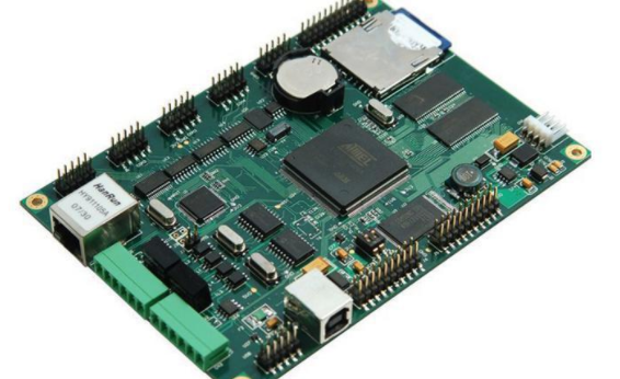
1. What is copper coating
The so-called copper pour is to use the unused space on the circuit board as a reference surface and then fill it with solid copper. These copper areas are also called copper filling.
The significance of copper coating is to reduce the impedance of the ground wire and improve the anti-interference ability; reduce the voltage drop and improve the efficiency of the power supply; when connected to the ground wire, it can also reduce the loop area.
Also for the purpose of making the PCB as non-deformed as possible during soldering, most PCB manufacturers will also require PCB designers to fill the open area of the PCB with copper or grid-like ground wires. If the copper is not handled properly, it will If the gain is not worth the loss, is the copper coating "more advantages than disadvantages" or "disadvantages more than advantages"?
Everyone knows that under high frequency, the distributed capacitance of the wiring on the printed circuit board will play a role. When the length is greater than 1/20 of the corresponding wavelength of the noise frequency, an antenna effect will occur, and the noise will be emitted through the wiring. If there is a poorly grounded copper pour in the PCB, the copper pour becomes a tool for spreading noise.
Therefore, in a high-frequency circuit, do not think that the ground wire is connected to the ground somewhere. This is the "ground wire". It must be less than λ/20 to punch holes in the wiring. The ground plane of the laminate is "good ground". If the copper coating is handled properly, the copper coating not only increases the current, but also plays a dual role of shielding interference.
2, two forms of copper coating
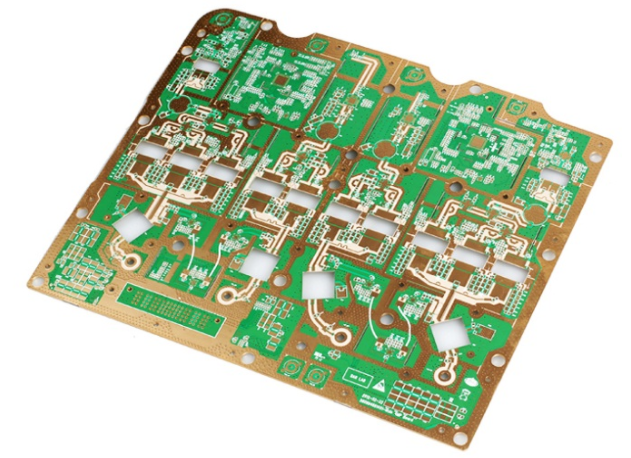
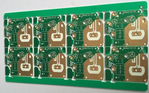
There are generally two basic methods for copper coating, namely large-area copper coating and grid copper. It is often asked whether large-area copper coating is better than grid copper coating. It is not good to generalize.
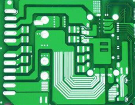
why? Large-area copper coating has the dual functions of increasing current and shielding. However, if large-area copper coating is used for wave soldering, the board may lift up and even blisters. Therefore, for large-area copper coating, several grooves are usually opened to relieve the blistering of the copper foil. As shown below:

The pure copper-clad grid is mainly used for shielding, and the effect of increasing the current is reduced. From the perspective of heat dissipation, the grid is good (it reduces the heating surface of the copper) and plays a role of electromagnetic shielding to a certain extent. Especially for circuits such as touch.
It should be pointed out that the grid is made up of traces in staggered directions. We know that for the circuit, the width of the trace has a corresponding "electrical length" for the operating frequency of the circuit board (the actual size is divided by The digital frequency corresponding to the working frequency is available, see related books for details).
When the operating frequency is not very high, perhaps the effect of the grid lines is not very obvious. Once the electrical length matches the operating frequency, it is very bad. You will find that the circuit does not work properly at all, and the system is emitting interference everywhere. signal of.
The suggestion is to choose according to the working condition of the designed circuit board, don't hold on to one thing. Therefore, high-frequency circuits have high requirements for multi-purpose grids against interference, and low-frequency circuits have circuits with large currents, such as commonly used complete copper.