Techniques and methods of high frequency PCB design
1. The corner of the transmission line should be 45° to reduce the return loss.
2. Use high-performance insulated circuit boards whose insulation constant values are strictly controlled by level. This method is conducive to effective management of the electromagnetic field between the insulating material and the adjacent wiring.
3. To improve the PCB design specifications related to high-precision etching. It is necessary to consider the total error of the specified line width of +/-0.0007 inches, manage the undercut and cross section of the wiring shape, and specify the plating conditions of the wiring sidewall. The overall management of wiring (wire) geometry and coating surface is very important to solve the skin effect problem related to microwave frequency and realize these specifications.

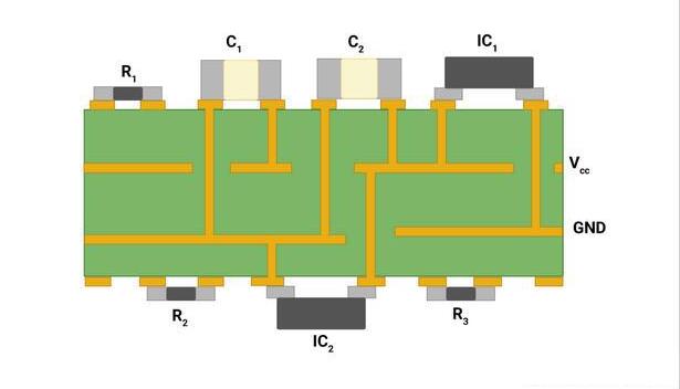
4. The protruding leads have tap inductance, so avoid using components with leads. In high frequency environments, it is best to use surface mount components.
5. For signal vias, avoid using a via processing (pth) process on sensitive boards, because this process will cause lead inductance at the vias.
6. Provide abundant ground planes. Use molded holes to connect these ground planes to prevent the 3D electromagnetic field from affecting the circuit board.
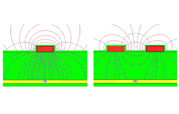
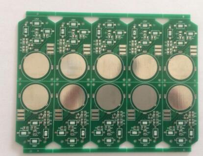
7. To choose electroless nickel plating or immersion gold plating process, do not use HASL method for electroplating. This kind of electroplated surface can provide better skin effect for high frequency current (Figure 2). In addition, this highly solderable coating requires fewer leads, which helps reduce environmental pollution.
8. The solder mask can prevent the flow of solder paste. However, due to the uncertainty of the thickness and the unknown of the insulation performance, the entire surface of the board is covered with solder mask material, which will cause a large change in the electromagnetic energy in the microstrip design. Generally, a solder dam is used as the solder mask. The electromagnetic field. In this case, we manage the conversion from microstrip to coaxial cable. In the coaxial cable, the ground layer is interwoven ring-shaped and evenly spaced. In microstrip, the ground plane is below the active line. This introduces some edge effects, which need to be understood, predicted and considered during design. Of course, this mismatch will also cause return loss, and this mismatch must be minimized to avoid noise and signal interference.
iPCB is a high-tech manufacturing enterprise focusing on the development and production of high-precision PCBs. iPCB is happy to be your business partner. Our business goal is to become the most professional prototyping PCB manufacturer in the world. Mainly focus on microwave high frequency PCB, high frequency mixed pressure, ultra-high multi-layer IC testing, from 1+ to 6+ HDI, Anylayer HDI, IC Substrate, IC test board, rigid flexible PCB, ordinary multi-layer FR4 PCB, etc. Products are widely used in industry 4.0, communications, industrial control, digital, power, computers, automobiles, medical, aerospace, instrumentation, Internet of Things and other fields.