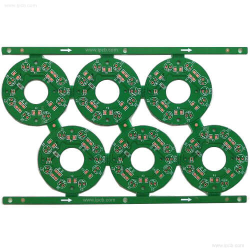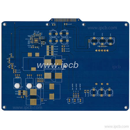
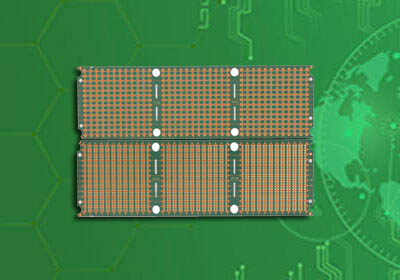
 Antenna PCB")
Material :2layers Halogen Free(HF) Antenna PCB
Material : FR-4
D K : 4.2
Layer:2Layers
Finished Thickness :0.8mm
Material Copper Thickness :0.5OZ
Finished Copper Thickness :1OZ(35μm)
SurfaceTreatment :Immersion Gold
Color : Green /White
Min Trace / Space:12mil/12mil
Special requirements : stable dielectric constant of material and strict line tolerance are required
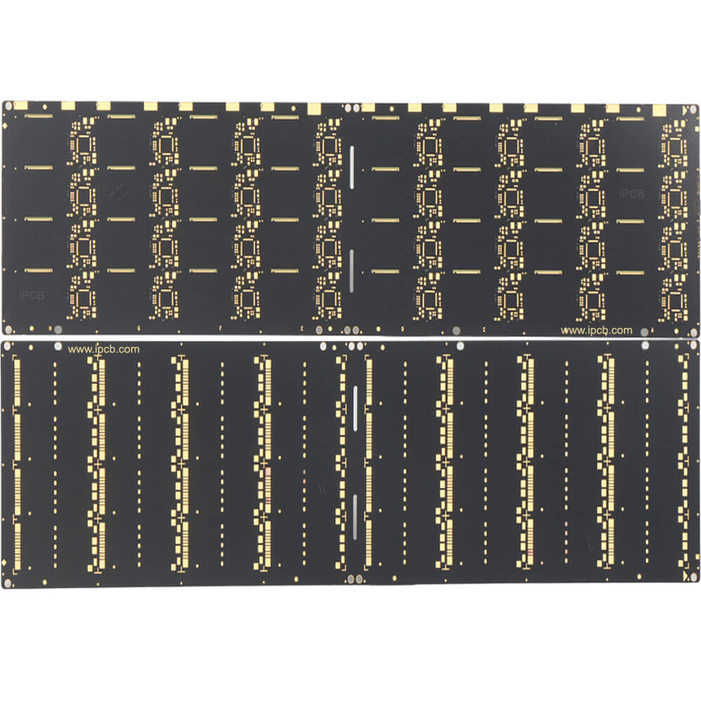
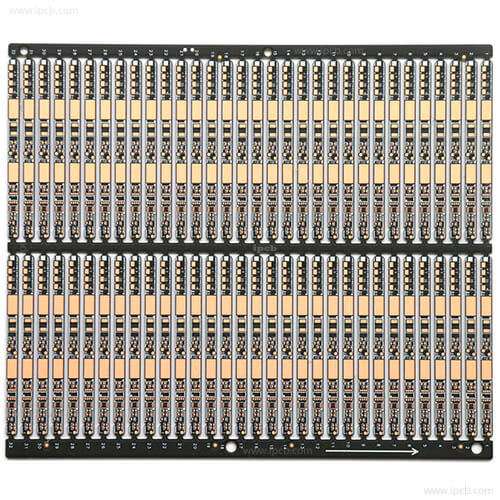
This is 2layers halogen free(HF) antenna PCB, antenna PCB has strict requirements on the line tolerance of radio frequency PCB(RF PCB) line. ipcb has sufficient experience to control the strict requirements of radio frequency(RF) antenna PCB.
PCB antenna refers to the part of PCB used for wireless receiving and transmitting. Most of PCB antenna is omnidirectional wireless transmitting and receiving antenna, but different from conventional antenna, it is on PCB plane.

Antenna PCB
Antenna PCB wireless equipment receiving and transmitting signals has been widely used in telecommunications. With the advent of 5g network, more and more electronic devices need antenna PCB communication, which is called the Internet of things (IOT).
Antenna PCB design and RF layout are the two most important components of any wireless device. You can use two identical RF products, each with a different PCB antenna design and layout, and get two distinct RF performance ranges. What's the difference between them? It all depends on the quality and considerations in the design process.
For many electronic applications in the 2.4 GHz and 915 MHz bands for commercial and consumer use, the demand for compact PCB antenna operation is increasing in ISM frequency band. As the name implies, the PCB antenna is printed directly on the PCB.

Cost optimized planar F-antenna PCB
Use the following formula to calculate the width of the antenna

Design of F-type antenna
The length of the meandering inverted-F antenna or mifa needs to be adjusted to consider the radiation impedance and frequency of the antenna. The tip and length of the mifa antenna are determined by the thickness of the PCB as follows:

Antenna PCB material should have high frequency, generally FR4 does not have good performance. Here we list the materials that can be used in antenna PCB manufacturing:
Rogers PCB,Teflon PCB,Arlon PCB,Taconic PCB,Nelco PCB,Fr5 PCB,Dupont PCB,Isola PCB
Material :2layers Halogen Free(HF) Antenna PCB
Material : FR-4
D K : 4.2
Layer:2Layers
Finished Thickness :0.8mm
Material Copper Thickness :0.5OZ
Finished Copper Thickness :1OZ(35μm)
SurfaceTreatment :Immersion Gold
Color : Green /White
Min Trace / Space:12mil/12mil
Special requirements : stable dielectric constant of material and strict line tolerance are required
For PCB technical problems, iPCB knowledgeable support team is here to help you with every step. You can also request PCB quotation here. Please contact E-mail sales@ipcb.com
We will respond very quickly.