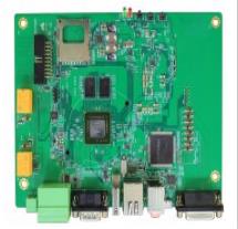
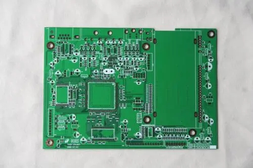
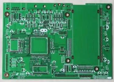
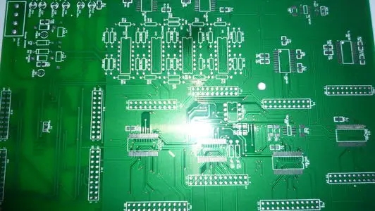
When designing a PCB, we often rely on experience and skills that we would normally find online. Each PCB design can be optimized for a specific application, and generally, its design rules apply only to the target application. For example, analog-to-digital converter PCB rules do not apply to RF PCBS and vice versa. However, certain guidelines can be considered universal to any PCB design. Here, in this tutorial, we will cover some basic questions and tricks that can significantly improve PCB design.

Power and signal distribution
Distribution is a key element in any electrical design. All of your components rely on power to function. Depending on your design, certain components may have power connections, while certain components on the same board may have poor power connections. For example, if all components were powered by a single wire, different impedances would be observed for each component, resulting in multiple grounding references. For example, if you have two ADC circuits, one at the beginning and one at the end, and both ADCs read an external voltage, each analog circuit will read a different potential relative to itself.
We can summarize the power distribution in three possible ways: single point source, star source, and multi-point source.
(a) Single point power supply: The power supply and ground wire of each component are separated from each other. The power cables of all components meet only at a single reference point. A single point is considered suitable for power. However, this is not feasible for complex or large/medium projects.
(b) Star source: Star source can be regarded as an improvement on a single point source. It is different because of its key feature: the wiring length between components is the same. Star connections are commonly used for complex high-speed signal boards with various clocks. In a high-speed signal PCB, the signal usually comes from the edge and then goes to the center. All signals can be transmitted from the center to any region of the board, and there is a delay between regions.(c) Multi-point sources: they are considered to be poor in any case. However, it is easy to use in any circuit. Multiple point sources may produce reference differences between components and in common impedance coupling. This design style also allows high-switching IC, clock and RF circuits to introduce noise into nearby circuits that share connections.
Of course, in our daily lives, we will not always have a single type of distribution. A compromise can be achieved by mixing single-point sources with multi-point sources. You can put analog sensitive devices and high speed/RF systems in one point, and all the other less sensitive peripherals in one point.
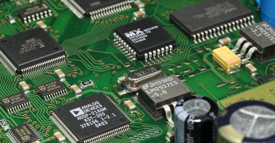
Power plane
Have you ever wondered if you should use a powered plane? The answer is yes. The power board is one of the ways to transfer power and reduce noise in any circuit. The power plane shortens the ground path, reduces inductance, and improves electromagnetic compatibility (EMC) performance.Thanks to the two power planes, a parallel plate decoupling capacitor is created to prevent noise propagation.
The power board also has an obvious advantage: due to its larger area, it allows greater current to flow through, thus increasing the PCB's operating temperature range. But please note: the power layer can improve the operating temperature, but wiring must also be considered. The tracking rules are given by IPC-2221 and IPC-9592
For PCBS with RF sources (or any high-speed signal application), you must have a complete grounding to improve board performance. The signals must be on different planes, and it is almost impossible to meet both requirements with two layers. If you want to design an antenna or any RF board with low complexity, you can use two layers.
In mixed-signal designs, manufacturers usually recommend separating analog ground from digital ground. Sensitive analog circuits are susceptible to high-speed switches and signals. If analog and digital grounding are different, the grounding plane will be separate. However, it has the following disadvantages. We should pay attention to the area of crosstalk and loop that divides the ground mainly caused by discontinuity of the ground plane. The figure below shows an example of two separate grounding planes. On the left side, the return current cannot pass directly along the signal line, so the loop region appears instead of the loop region on the right.