How to solve the EMI problem in PCB multi-layer circuit board design
There are many ways to solve EMI problems. Modern EMI suppression methods include: using EMI suppression coatings, selecting appropriate EMI suppression parts, and EMI simulation design. This article starts from the basic circuit board layout, the following editor from Shenzhen circuit board manufacturer discusses the role and design techniques of PCB multilayer circuit board layered stacking in controlling EMI radiation.
power bus
Properly placing a capacitor of appropriate capacity near the power supply pin of the IC can make the IC output voltage jump faster. However, the problem does not end here. Due to the limited frequency response of the capacitor, the capacitor cannot generate the harmonic power required to drive the IC output cleanly in the full frequency band. In addition, the transient voltage formed on the power bus will form a voltage drop across the inductance of the decoupling path, and these transient voltages are the main common mode EMI interference sources. How should we solve these problems?
As far as the IC on our circuit board is concerned, the power layer around the IC can be regarded as an excellent high-frequency capacitor, which can collect the part of the energy leaked by the discrete capacitor that provides high-frequency energy for clean output. In addition, the inductance of a good power layer should be small, so the transient signal synthesized by the inductance is also small, thereby reducing common mode EMI.

Of course, the connection between the power layer and the IC power pin must be as short as possible, because the rising edge of the digital signal is getting faster and faster, and it is best to connect it directly to the pad where the IC power pin is located. This needs to be discussed separately.
In order to control common-mode EMI, the power plane must help decoupling and have a sufficiently low inductance. This power plane must be a well-designed pair of power planes. Someone may ask, how good is good? The answer to the question depends on the layering of the power supply, the material between the layers, and the operating frequency (that is, a function of the IC rise time). Usually, the spacing of the power layer is 6mil, and the interlayer is FR4 glass fiber board material, the equivalent capacitance per square inch of the power layer is about 75pF. Obviously, the smaller the layer spacing, the greater the capacitance.
There are not many devices with a rise time of 100 to 300 ps, but according to the current IC development speed, devices with a rise time in the range of 100 to 300 ps will occupy a high proportion. For circuits with a rise time of 100 to 300ps, 3mil layer spacing will no longer be suitable for most applications. At that time, it was necessary to adopt a layering technology with a layer spacing of less than 1 mil, and use a material with a high dielectric constant to replace the FR4 glass fiber board dielectric material. Now, ceramics and ceramic plastics can meet the design requirements of 100 to 300 ps rise time circuits.
Although new materials and new methods may be used in the future, for today’s common 1 to 3ns rise time circuits, 3 to 6mil layer spacing and FR4 dielectric materials, it is usually sufficient to handle high-end harmonics and make the transient signal low enough, that is to say, Common mode EMI can be reduced very low. The PCB layered stacking design examples given in this article will assume a layer spacing of 3 to 6 mils.
Electromagnetic shielding
From the perspective of signal traces, a good layering strategy should be to put all signal traces on one or several layers, and these layers are next to the power layer or ground layer. For the power supply, a good layering strategy should be that the power layer is adjacent to the ground layer, and the distance between the power layer and the ground layer is as small as possible. This is what we call the "layering" strategy.
PCB circuit board stacking
What stacking strategy helps to shield and suppress EMI? The following layered stacking scheme assumes that the power supply current flows on a single layer, and the single voltage or multiple voltages are distributed in different parts of the same layer. The case of multiple power layers will be discussed later.
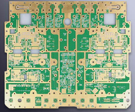
4-layer circuit board
There are several potential problems with the 4-layer circuit board design. First of all, the traditional four-layer board with a thickness of 62 mils, even if the signal layer is on the outer layer, and the power and ground layers are on the inner layer, the distance between the power layer and the ground layer is still too large.
If the cost requirement is first, you can consider the following two traditional 4-layer board alternatives. Both of these solutions can improve the performance of EMI suppression, but they are only suitable for applications where the component density on the board is low enough and there is enough area around the components (place the required power supply copper layer).
The first is the preferred solution. The outer layers of the PCB circuit board are all ground layers, and the middle two layers are signal/power layers. The power supply on the signal layer is routed with a wide line, which can make the path impedance of the power supply current low, and the impedance of the signal microstrip path is also low. From the perspective of EMI control, this is the best 4-layer PCB structure available. In the second scheme, the outer layer uses power and ground, and the middle two layers use signals. Compared with the traditional 4-layer board, the improvement is smaller, and the interlayer impedance is as poor as the traditional 4-layer board.
If you want to control the trace impedance, the above stacking scheme must be very careful to arrange the traces under the power and ground copper islands. In addition, the copper islands on the power supply or ground layer should be interconnected as much as possible to ensure DC and low-frequency connectivity.
6-layer circuit board
If the component density on a 4-layer circuit board is relatively high, a 6-layer board is best. However, in the design of the 6-layer circuit board, some stacking schemes are not good enough to shield the electromagnetic field, and have little effect on the reduction of the transient signal of the power bus. Two examples are discussed below.
In the first example, the power supply and ground are placed on the 2nd and 5th layers respectively. Due to the high copper impedance of the power supply, it is very unfavorable to control the common mode EMI radiation. However, from the point of view of signal impedance control, this method is very correct.
In the second example, the power supply and ground are placed on the 3rd and 4th layers respectively. This design solves the problem of power supply copper impedance. Due to the poor electromagnetic shielding performance of the 1st and 6th layers, the differential mode EMI is increased. If the number of signal lines on the two outer layers is the least, and the trace length is very short (shorter than 1/20 of the wavelength of the highest harmonic of the signal), this design can solve the differential mode EMI problem. Fill the copper-clad area with no components and no traces on the outer layer and ground the copper-clad area (every 1/20 wavelength as an interval), which is particularly good at suppressing differential mode EMI. As mentioned earlier, it is necessary to connect the copper area with the internal ground plane at multiple points.
.