A step-down switching power supply schematic for consumer electronics applications. The designer shall be able to distinguish on this circuit diagram the components of the power circuit from those of the control signal circuit. The problem can be serious if the designer treats all the components of the power supply as if they were components of a digital circuit. It is usually necessary first to know the path of the high frequency PCB current of the power supply, and to distinguish between the small signal control circuit and the power circuit components and their wiring.
Generally speaking, the power circuit of the power supply mainly includes the input filter capacitor, output filter capacitor, filter inductor, and upper and lower power feTS. The control circuit mainly includes PWM control chip, bypass capacitor, bootstrap circuit, feedback voltage divider and feedback compensation circuit.

A typical step-down switching power supply schematic (12V input, 3.3V/15A output) [power control circuit (thin line), power circuit (thick line)] Power supply power circuit PCB layout
The correct placement and wiring of power supply devices on the PCB will determine whether the whole power supply works properly. Designers must first understand the waveform of voltage and current on switching power supply power devices.
The following shows the current and voltage waveforms on the power circuit components of a step-down switching power supply.
Since the current flowing through the input filter capacitor (Cin), the upper mosFEts (S1) and the lower MOSfets (S2) is ac current with high frequency and peak value, the loop area formed by CIN-S1-S2 should be minimized. At the same time, the loop area composed of S2, L and output filter capacitor (Cout) should be minimized.
Switching power The current and voltage in the circuit
If a designer fails to make a power circuit PCB as outlined in this article, it is likely to make the wrong power PCB as shown below.
Incorrect switching power supply power device placement and wiring
There are many errors in this PCB layout:
Due to the large ESL of Cin, the high frequency filtering ability of Cin basically disappears; Second, the area of CIN-S1-S2 and S2-L-Cout loops is too large, and the electromagnetic noise generated will cause great interference to the power supply itself and surrounding circuits. Third, the pads of L are too close to each other, resulting in CP being too large and reducing its high-frequency filtering function; Fourth, the Cout pad lead is too long, resulting in THE LOSS of the HIGH frequency filtering function of THE ESL is too large.
This is a better power circuit for PCB wiring. The area of cIN-S1-S2 and S2-L-Cout loops has been controlled.
The connection between the source of S1, the drain of S2 and L is a single piece of copper pad. Because the voltage at this connection point is high frequency, S1, S2 and L need to be very close together. Although the wiring between L and Cout has no high frequency current with peak value, the wider wiring can reduce the loss of DC impedance and improve the efficiency of the power supply.
If cost allows, the power supply can be a PCB with two sides completely connected to the ground, but care must be taken to avoid power and signal lines on the ground. A chip capacitor is added to the input and output ports of the power supply to improve the high frequency filtering performance of the power supply.
Power control circuit PCB layout
PCB layout of power control circuits is also very important. Unreasonable layout will cause the power supply output voltage drift and oscillation. The control line should be placed on the edge of the power circuit, not in the middle of the HIGH frequency AC loop. The bypass capacitor should be close to the VCC and GND of the chip. A feedback divider resistor is also plac
ed near the chip. The loop that drives the chip to the MOSFEts should also be kept as short as possible.
Basic points of power layout: the drive circuit loop from the control chip to the upper and lower fET should be as short as possible.
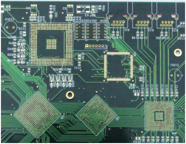
PCB layout example of switching power supply
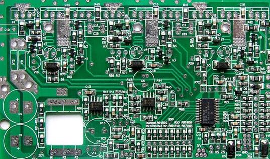
We see in the article that the typical step-down switching power supply PCB component surface map. A low-cost PWM controller (Semtech SC1104A) is used in this power supply. The lower layer of PCB is a complete ground layer. There is no separation between the PCB power formation and the control formation.
It can be seen that the power circuit of the power supply from the input socket (upper left of PCB) through the input filter capacitor (C1, C2), S1, S2, L1, output filter capacitor (C10, C11, C12, C13), all the way to the output socket (lower right of PCB). The SC1104A is placed at the bottom left of the PCB.
Since the power circuit current does not pass through the control circuit at the layer, there is no need to separate the control circuit connection from the power circuit connection. If the input socket is placed at the bottom left of the PCB, the
8 big takeaways:
1. The capacitance of the bypass chip capacitor should not be too large, and its parasitic series induction should be as small as possible. Multiple capacitors in parallel can improve the impedance characteristics of the capacitor;
2. The parasitic shunt capacitance of the inductor should be as small as possible, and the distance between the inductor pins and pads should be as far as possible;
3. Avoid placing any power or signal wiring on the stratum;
4. The area of high-frequency loop should be reduced as much as possible;
5. Hole placement should not destroy the path of high frequency current on the formation;
6. Different circuits on the system board need different grounding, and the grounding of different circuits is connected with the power supply grounding through a single point;
7. the control chip to the upper and lower end of the field effect tube drive circuit loop should be as short as possible;
8. Switching power supply power circuit and control signal circuit components need to be connected to different ground layers. These two ground layers are generally connected through a single point