Which aspects should the circuit board DEBUG start from?

As far as digital circuits are concerned, first determine three things in order
Confirm that all power supply values meet the design requirements. Some systems with multiple power supplies may require certain specifications for the order and speed of the power supplies.
Confirm that all clock signal frequencies are working properly and there are no non-monotonic problems on the edges of the signal.
Confirm whether the reset signal meets the specification requirements.
If these are normal, the chip should send out a cycle signal. Next, debug according to the operating principle of the system and the bus protocol.
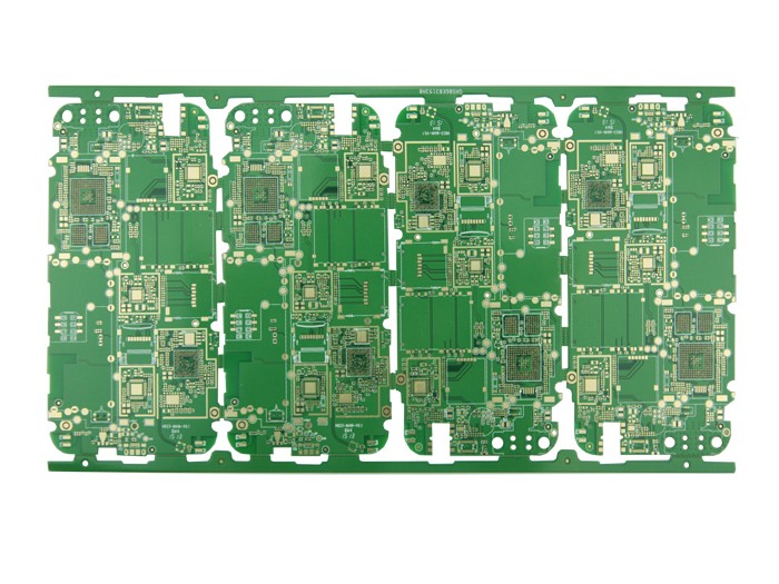
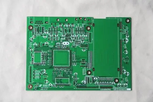
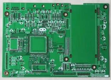
21. In the case of a fixed circuit board size, if the PCB design needs to accommodate more functions, it is often necessary to increase the PCB trace density, but this may increase the mutual interference of the traces, and at the same time, the traces are too thin and the impedance Can't reduce, please introduce the skills in high-speed (>100MHz) high-density PCB design?
When designing high-speed PCBs and high-density PCBs, crosstalk interference (crosstalk interference) really needs special attention, because it has a great impact on timing and signal integrity. Here are some points to note: 1). Control the continuity and matching of the characteristic impedance of the trace. 2). The size of the trace spacing. The commonly seen spacing is twice the line width. The effect of the trace spacing on the timing and signal integrity can be known through simulation, and the tolerable small spacing can be found. The result of different chip signals may be different. 3). Choose the appropriate termination method. 4). Avoid two adjacent layers with the same wiring direction, even if there are wirings that overlap up and down, because this kind of crosstalk is greater than that of adjacent wiring on the same layer. 5). Use blind/buried vias to increase the trace area. However, the manufacturing cost of the PCB board will increase.
It is indeed difficult to achieve complete parallelism and equal length in actual implementation, but it is still necessary to do it as much as possible. In addition, differential termination and common mode termination can be reserved to alleviate the impact on timing and signal integrity.