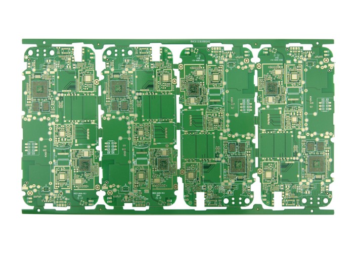
The basic requirement for etching quality is to be able to completely remove all the copper layers except under the resist layer, and that's it. Strictly speaking, if it is to be accurately defined, then the etching quality must include the consistency of the wire width and the degree of undercutting. Due to the inherent characteristics of the current etching solution, which not only produces an etching effect on the downward direction but also on the left and right directions, side etching is almost inevitable.

The problem of side etching is a frequently discussed item in the etching parameters. It is defined as the ratio of the width of the side etching to the depth of the etching, which is called the etching factor. In the printed circuit industry, it has a wide range of changes, from 1:1 to 1:5. Obviously, a small undercut degree or a low etching factor is satisfactory.
The structure of the etching equipment and the etching solutions of different compositions will affect the etching factor or the degree of side etching, or in optimistic terms, it can be controlled. The use of certain additives can reduce the degree of side erosion. The chemical composition of these additives is generally a trade secret, and the respective developers do not disclose it to the outside world. As for the structure of the etching equipment, the following chapters will be specifically discussed.
From many aspects, the quality of etching has existed long before the printed board entered the etching machine. Because there are very close internal connections between the various processes or processes of printed circuit processing, there is no process that is not affected by other processes and does not affect other processes. Many of the problems identified as etching quality actually existed in the process of removing the film or even before. As for the etching process of the outer layer graphics, because the "inverted stream" it embodies is more prominent than most printed board processes, many problems are reflected on it. At the same time, this is also because the etching is the last step in a long series of processes starting from the self-adhesive film and photosensitive, after which the outer layer pattern is successfully transferred. The more links, the greater the possibility of problems. This can be seen as a very special aspect of the printed circuit production process.
In theory, after the printed PCB circuit enters the etching stage, the cross-sectional state of the figure should be as shown in Figure 2. In the process of processing printed circuits by pattern electroplating, the ideal state should be: the total thickness of the electroplated copper and tin or copper and lead tin should not exceed the thickness of the electroplating resistant photosensitive film, so that the electroplated pattern is completely covered on both sides of the film. The "wall" blocks and is embedded in it. However, in actual production, after electroplating printed circuit boards all over the world, the plating pattern is much thicker than the photosensitive pattern. In the process of electroplating copper and lead-tin, because the plating height exceeds the photosensitive film, a tendency of lateral accumulation occurs, and the problem arises from this. The tin or lead-tin resist layer covering the lines extends to both sides to form an "edge", covering a small part of the photosensitive film under the "edge" (see Figure 5).
The "edge" formed by tin or lead tin makes it impossible to completely remove the photosensitive film when removing the film, leaving a small part of the "residual glue" under the "edge" (see Figure 6). The "residual glue" or "residual film" left under the "edge" of the resist will cause incomplete etching. The lines formed "copper roots" on both sides after etching. The copper roots narrowed the line spacing, causing the printed board to not meet the requirements of Party A, and may even be rejected. Rejection will greatly increase the production cost of PCB. In addition, in many cases, due to the formation of dissolution due to the reaction, in the printed circuit industry, the residual film and copper may also form and accumulate in the corrosive liquid and be blocked in the nozzle of the corroding machine and the acid-resistant pump, and it has to be shut down for processing and cleaning., Which affects work efficiency.
The above is an introduction to the etching quality and pre-existing problems in the etching of PCB outer circuit. Ipcb also provides PCB manufacturers and PCB manufacturing technology.