Overview of electrical reliability in PCBA processing
At present, the country has higher and higher requirements for environmental protection and greater efforts in link governance. This is a challenge but also an opportunity for PCB factories. If PCB factories are determined to solve the problem of environmental pollution, then FPC flexible circuit board products can be at the forefront of the market, and PCB factories can get opportunities for further development.
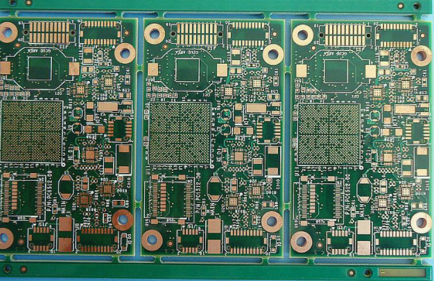
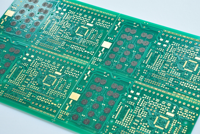
The same PCB circuit board generally needs to be processed by SMT, and then flow soldering, wave soldering, rework and other processes. It is likely to form different residues. In a humid environment and a certain voltage, it can react electrochemically with electrical conductors., Resulting in a decrease in surface insulation resistance (SIR). If electromigration and dendritic growth occur, there will be a short circuit between the wires, causing electromigration risk (commonly known as "leakage").
In order to ensure electrical reliability, it is necessary to evaluate the performance of different non-cleaning fluxes. Try to use the same flux for the same PCB, or clean it after soldering.

According to the reliability analysis of the mechanical strength of the solder joints, tin whiskers, pores, cracks, intercellular compounds, mechanical vibration failure, thermal cycle failure, electrical reliability, any failure is more likely to occur in the solder joints with the following defects: Thickness is too thin and too thick After welding: there are pores and micro-cracks in the solder joint or interface; the wetting area of the solder joint is small (the bonding size of the component welding end and the pad is too small): the microstructure of the solder joint is not dense, and the crystalline particles Large, large internal stress. Some defects can be detected by visual inspection, AOI and X-ray. For example, the overlap size of the solder joints is small, the surface of the solder joints has pores, and the cracks are more obvious.
However, the microstructure, internal stress, internal voids and cracks of the solder joints, especially the thickness of intermetallic compounds, these hidden defects are invisible to the naked eye, and cannot be detected by manual or automatic inspection through SMT processing. The test requires various reliability tests and analyses, such as temperature cycle test, vibration test, drop test, high temperature storage test, damp heat test, electromigration test, high accelerated life test and high accelerated stress screening; then electrical and mechanical properties ( Such as solder joint shear strength, tensile strength) test; finally through visual inspection, X-ray fluoroscopy, metallographic section, scanning electron microscope and other test analysis to make a judgment.
iPCB is happy to be your business partner. Our business goal is to become the most professional prototyping PCB manufacturer in the world. With more than ten years of experience in this field, we are committed to meeting the needs of customers from different industries in terms of quality, delivery, cost-effectiveness and any other demanding requirements. As one of the most experienced PCB manufacturers and SMT assemblers in China, we are proud to be your best business partner and good friend in all aspects of your PCB needs. We strive to make your research and development work easy and worry-free.