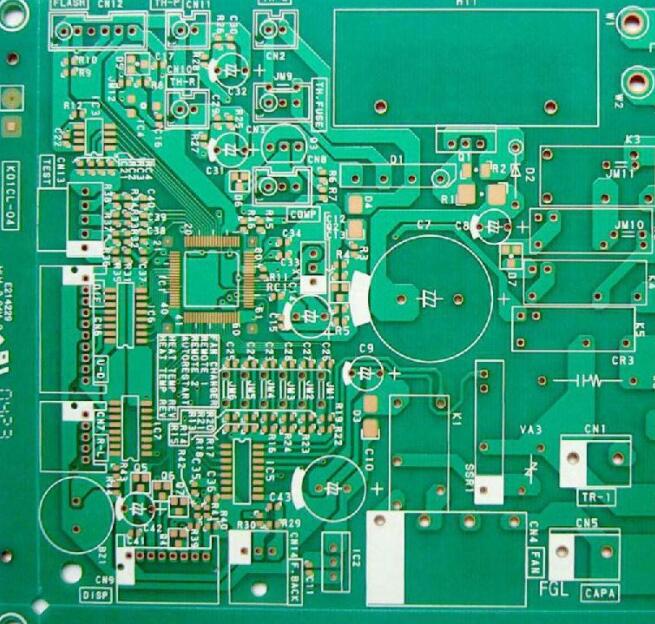
The basic electrical function of a printed circuit is to supply electrical energy to each electronic component and to transmit electrical signals from one electronic component to another electronic component (such as a transistor or an integrated circuit). With the rapid switching operation of transistors, the transistor needs to be turned on or cut off a large current instantaneously, and the power supply voltage fluctuates significantly, which easily affects the stable operation of the device. When working at low speed, only a simple electrical connection is required between the signal sending end (device) and the signal receiving end (device). However, when working at high speeds, the connection line (microstrip line) is required to have a special shape and length, as well as a special arrangement of power planes and ground planes, so that the transmitted signal does not have serious waveform distortion. Unless otherwise specified, the waveform of the signal transmitted from one end to the other must not be significantly altered. Transmission lines that take too long to transmit signals are not suitable for transmitting high-speed signals, because in the process of high-speed pulse transmission, it is possible that the pre-pulse has not reached the receiving end, but the secondary pulse has left the transmitting end. The higher the frequency, the more likely the signal will be intermodulation interference and electromagnetic interference, and the more difficult it will be to prevent the circuit from being subjected to signal intermodulation interference or electromagnetic interference. In order to stabilize the power supply, many decoupling capacitors are required between the power supply layer and the ground layer. The reasonable design of conductor pattern arrangement, layer structure and signal transmission line can reduce noise. In a multilayer PCB, the power supply surface should be close to the chip in order to reduce the power supply impedance. The structure of the power supply surface close to the wiring layer can effectively reduce the radiation noise.

Second, the printed circuit designer should first read the circuit schematic
If the designer of a printed circuit wants to design a circuit schematic into a qualified printed circuit, he must first understand the circuit schematic. The so-called understanding is not a designer who is demanding a printed circuit board, and is as proficient in circuit principles as a designer of circuit schematics, especially in the case of using computer-aided design (CAD) to design a printed circuit board. Basic knowledge of electronic circuits is sufficient. And for some unclear problems in the electronic circuit, you can communicate with the designer of the circuit schematic in time.
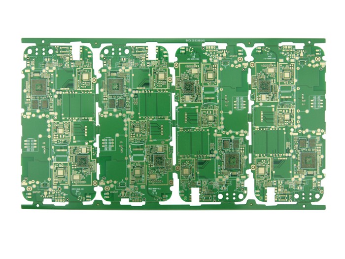
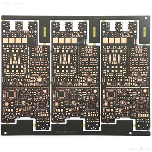
Three single-sided, double-sided and multi-layer PCB design procedures are quite different
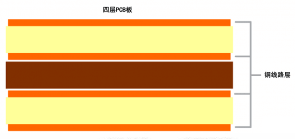
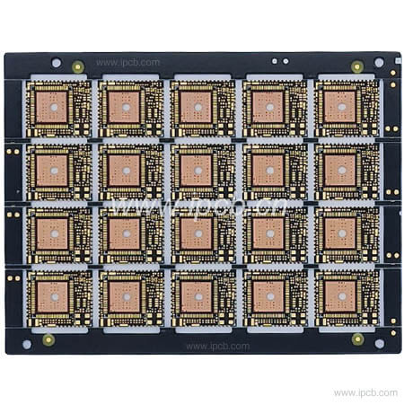
The manufacturing processes of single-sided printed circuit boards, double-sided printed circuit boards and multilayer printed circuit boards are quite different. Simply put, for single-sided printed circuit boards and double-sided printed circuit boards, you can first make a copper-clad board, then design the pattern of the printed circuit board, and selectively corrode the conductors (including pads) on the surface of the copper-clad board The graphics are made into a printed circuit board, that is to say, the design of the printed circuit board can be before the production of the copper-clad board, or after the production of the copper-clad board is completed. However, a multilayer printed circuit board must first produce an inner layer with a copper cylinder conductor pattern on the surface of the insulating substrate according to the design pattern of the printed circuit board, and then laminate them to form a printed circuit board. The whole of the printed circuit board, that is, the design of the multilayer PCB board must be arranged before the printed circuit board is manufactured.