To maintain PCB board signal integrity, a unique method of interconnecting layers (through-holes) to match printed line impedance should be used. As the speed of data communication increases to more than 3Gbps, signal integrity is crucial for the smooth transmission of data. Circuit board designers try to eliminate every impedance mismatch along a high-speed signal path because of these impedance mismatches
To maintain PCB signal integrity, a unique method of interconnecting layers (through-holes) to match printed line impedance should be used.

As the speed of data communication increases to more than 3Gbps, signal integrity is crucial for the smooth transmission of data. Circuit board designers try to eliminate every impedance mismatch in the path of high-speed signals, because these impedance mismatches can produce jitter and reduce the opening of data eyes -- thus not only shortening the distance of data transmission, It also minimizes the margin of general-purpose jitter specifications such as SONET (synchronous optical network) or XAUI (10Gb subsidiary cell interface).
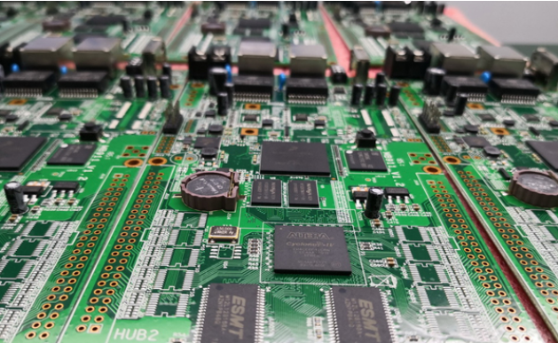
As the signal density on a printed circuit board increases, more signal transport layers are required, and transmission via interlayer interconnections (through-holes) is inevitable. In the past, through-holes have represented a significant source of signal distortion because their impedance is typically about 25 to 35 ω. Such a large impedance discontinuity would reduce the opening of the data eye map by 3dB and produce a lot of jitter depending on the data rate. As a result, circuit board designers either try to avoid the use of through-holes on high-speed lines or try new techniques, such as boring or blind holes. These methods, while useful, can add complexity and greatly increase board costs.
Both channels are only 2.8 inches long, but the effect of the through-hole is clearly visible. The conventional through hole (yellow curve) attenuates multiple frequencies, resulting in a smaller and slower rise time of the data graph than the impedance controlled through hole (green curve).

, impedance mismatch should be as small as possible. Even the mismatch will appear at a discrete frequency of the S21 curve and affect the signal quality. You can improve the performance of impedance controlled through-holes as long as you satisfy important design parameters such as spacing, printed line width and weld zone width. For example, the size of the concave edge (or gap) of the signal through hole is critical. It must be at least the difference between the distance A and the diameter D between the signal through hole and the ground through hole, so that the concave edge of the signal through hole can touch the ground through hole. Otherwise, the metal in the grounding layer, power layer, or both will get too close to the signal through-hole, generating unwanted additional capacitance and lowering the through-hole impedance below the calculated 50 ω.
Similarly, each through-hole connecting the top or bottom microstrip line to the inner microstrip line produces a stub transversal line. When the short transversal length is less than the signal rise time, the short transversal is almost imperceptible. If the short transversal length is long, considerable signal distortion can be caused. For example, a 40-mile-long stub has a signal running length of about 14ps in a system with a signal rise time of about 50ps and a signal rate of 3.125Gbps. In the bad case, the stub is a quarter of the wavelength of an important frequency, so the stub is short-circuited to that frequency, causing the original signal to disappear.
The above formulas assume that the diameter of the signal through hole and the ground through hole are the same. To use different diameters, you have to modify the capacitance formula. The designer should select the diameter of the through-hole according to the width of the printed line to be connected. If the printed line is much smaller than the through-hole, the transition from the 50 ω printed line to the through-hole weld zone will cause unwanted impedance discontinuities. The designer should also consider the distance between the ground through hole and the printed line to be connected. This becomes a problem when the distance between the ground through hole and the printed line is less than the distance between the printed line and the reference layer, resulting in additional printed line capacitance and thus reduced printed line impedance to less than 50 ω. For example, on the test board, the distance between the signal print line and the ground through-hole is about 11 mils, and the print line is about 10 mils above the ground reference layer.
Another important design consideration is the size of the weld zone, as each through-hole connecting the printed line requires a weld zone. The weld zone should be as small as possible because the distance from the weld zone to the ground through hole is less than the distance from the signal through hole to the ground through hole. Because of these zones, the distance is shortened, the capacitance is increased, and the total impedance is reduced.
In a typical design, there are not always four grounding through-holes. As long as the return current has a path from VDD to ground through a nearby by-pass capacitor, the through-hole configuration is as good as the power supply through-hole.
For example, now consider a circuit board that includes this through-hole configuration in a BGA output pin with a 1 mm grid. Since it is a fixed output pin, you can only ground the two external through holes; The other two through-holes are connected to the VDD. This through-hole structure works well because you can also connect the SMD bypass capacitor between the VDD and ground in the BGA.
You can also use this through-hole structure for differential signals. Differential signals can share two external through holes, saving board space. Texas Instruments has adopted this approach on the evaluation board for its XAUI transceivers because of the limited space within the BGA. For impedance-controlled through-holes, the size of the interlayer spacing does not matter because it is the grounded through-holes, not the metal layer, that form the capacitance. However, conventional through-holes depend on interlayer capacitance. Therefore, even if the thickness of the board does not change, you have to design special through holes for different layers of stacking.