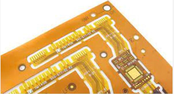
The flex PCB coverlay is a solid material consisting of two parts, including a layer of acrylic or epoxy-based flexible adhesive and a layer of polyimide. The adhesive bonds the polyimide into the flexible circuit and seals the circuit. Then, the flex PCB coverlay is aligned with the circuit surface and aligned at a specific temperature and pressure.

The flex PCB coverlay is a layer that protects the circuit board and copper foil. It has the same function as a solder mask but increases flexibility. Its thickness is usually one mil thick, but different thicknesses can meet the exact design requirements.
The coverlay can be used as a solder resist for flexible printed circuit boards. Traditional solder covers only have limited flexibility, so for flexible circuits that require greater flexibility, the cover layer adheres to protect the copper structure.
The Flex PCB coverlay consists of a solid sheet of polyimide and a layer of flexible adhesive. The covering layer and the solder mask layer on the rigid board have identical functions but are only applicable to flexible printed circuit board PCBs. Traditional solder mask boards only have limited flexibility, so for flexible circuits that require greater flexibility, the cover layer is bonded (glued) to encapsulate and protect the external copper circuit layer of flexible printed circuits (FPCs).
What is the difference between a flex PCB coverlay and a solder mask layer?
1. The flexible PCB coverlay is a combination of adhesive and Kapton (a polyimide), but the solder mask (solder mask) is liquid based.
2. The size of the overlay dam should be maintained at a minimum of 10 mils; However, the size of the welding dam should be maintained at a minimum of 4 mils. The dam prevents molten and liquefied solder from flowing from one pad to another nearby pad.
3. The marks on the opening of the cover layer mask can be close to 3 mils. However, using a 3mil solder mask may lead to edge-cutting or nonrecording issues (regarding the imaging of the solder mask). For resistance welding, it is recommended to maintain a minimum distance of 4 mils.
4. The markings covering the mask opening can be close to 3mil. However, using a 3mil solder mask may lead to edge or nonrecording issues (regarding solder mask imaging). For welding resistance, it is recommended to have a minimum distance of 4mil.
5. Unlike resistance welding, the covering layer cannot be used for pitch components.
The difference between flex PCB coverlay and rigid PCB solder mask film
Unlike rigid PCB solder mask films, the covering layer is usually provided in rolls, sometimes in sheets and cut into specific sizes. According to the complexity and feature size of flexible PCB design, the required cladding openings can be drilled, wired, punched, or laser cut. Once the pattern is formed, the film aligns with the copper circuit layer and is pressed under heating and pressure. Over time, the adhesive is cured to complete the bonding of the cover layer.
The flexible PCB overlay provides the same functionality as the solder mask used on rigid PCBs. However, compared to solder masks with limited flexibility, flexible PCB coverlay provides more durability and flexibility, which is very important in the application of flexible printed circuits.
In the manufacturing process of flexible PCBs, a flexible PCB coverlay is applied to encapsulate and protect the copper structure (external circuits and wiring) of the flexible PCB. It is a kind of covering film, which is composed of a thick acrylic or polyimide sheet and a flexible adhesive layer. The adhesive layer is laminated at high temperatures and then pressurized to the circuit surface. The main function of flexible PCB sheaths is to protect the base of flexible printed circuit materials. It has high-temperature resistance and can be used for heaters and ovens.
The main function of a flexible PCB board is to protect the circuits on the flexible PCB board. It serves as a flexible printed circuit board for solder resist or solder film. Traditional solder mask or solder mask has limited ductility or flexibility. Therefore, for flexible printed circuits that require greater flexibility, a flexible PCB coverlay should be pasted on the circuit board to protect copper foil and wires. The flexible PCB overlay is commonly used in the PCB industry and is also the preferred solution for the external circuit packaging layer of flexible printed circuits. It provides a more durable and powerful solution with excellent flexibility and high Dielectric strength.
The flexible PCB coverlay provides effective protection and insulation for the outer circuit of the flexible PCB, which can meet various design requirements. It is equally important to understand the differences between the overlay and solder mask layers to promote flexible PCB design.