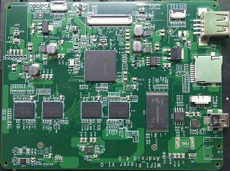
With the development of electronic products to high density and high precision, the same requirements are put forward on circuit boards accordingly. The most effective way to increase PCB density is to reduce the number of through holes, and accurately set blind holes and buried holes.
Blind hole board production knowledge of circuit board
1. Blind hole definition
a: In contrast to through holes, through holes refer to holes drilled through each layer, and blind holes are non-drilled through holes. (Illustration, eight-layer board example: through hole, blind hole, buried hole) b: Blind hole subdivision: BLIND HOLE, BURIED HOLE (outer layer is not visible); c: From the production process Distinction: Blind holes are drilled before pressing, and through holes are drilled after pressing.
2. Production Method
A: Drill belt:
(1): Select reference point: Select the through hole (ie a hole in the first drilled belt) as the unit reference hole.
(2): Each blind hole drilling belt needs to select a hole and mark its coordinates relative to the unit reference hole.
(3): Note that which drill belt corresponds to which layers: the unit sub-hole diagram and drill tip table must be marked, and the names of the front and back must be consistent; the sub-hole diagram cannot appear with abc, and the front is 1st, 2nd Indicates the situation.
Note that when the laser hole is sleeved with the inner buried hole, that is, the holes of the two drill belts are in the same position, you need to ask the customer to move the position of the laser hole to ensure the electrical connection.
B: Production pnl board edge process hole:
Ordinary multi-layer board: the inner layer is not drilled;
(1): Rivets gh, aoi gh, et gh are all shot after eroding the board (beer out)
(2): target hole (drilled hole gh) ccd: the outer layer needs to be copper out, x-ray machine: directly punch out, and note that the long side is at least 11 inches.
Blind hole plate:
All tooling holes are drilled, pay attention to rivets gh; need to be out to avoid misalignment.
(aoi gh is also a beer), the edge of the pnl board needs to be drilled to distinguish each board.

3. Film modification:
(1): Indicate that the film produces positive and negative films:
General principle: The board thickness is greater than 8mil (without copper) and the positive film process is adopted;
The thickness of the board is less than 8mil (without copper) and the negative film process (thin board);
Line thickness When the line gap valley is large, the copper thickness at d/f should be considered, not the bottom copper thickness.
The blind hole ring can be made 5mil, no need to make 7mil.
The inner independent pad corresponding to the blind hole needs to be retained.
Blind holes cannot be made without ring holes.
4. Process:
The buried-hole plate is the same as the ordinary double-sided board.
Blind hole plate, that is, one side is the outer layer:
Positive film process: Single-sided d/f is required, and attention must be paid not to roll the wrong side (when the double-sided bottom copper is inconsistent); when d/f is exposed, the glossy copper surface is covered with black tape to prevent light transmission.
Because the blind hole board is made more than two times, the thickness of the finished product is very easy to be too thick. Therefore, the thickness of the board should be controlled and the range of copper thickness should be indicated after etching.
After pressing the board, use the x-ray machine to punch out the target holes for the multilayer board.
Negative film process: for thin plates (<12mil with copper) because they cannot be produced in the drawing circuit, they must be produced in the hydrometal drawing, and the hydro drawing cannot separate the current, so it is not possible to do single-sided non-current or drawing according to the mi requirements. Small current. If the positive film process is used, the copper thickness on one side is often too thick, causing etching difficulties and the phenomenon of thin lines. Therefore, this type of board needs to use the negative film process.
5. The drilling sequence of through holes and blind holes is different, and the deviation is inconsistent during production
Blind hole plates are more prone to deformation, and it is difficult to open horizontal and straight materials to control multi-layer board alignment and tube spacing. Therefore, only open horizontal or only straight materials when cutting.
6. Laser drill
LASER DRILL is a kind of blind hole with its own characteristics:
Aperture size: 4-6 mil
pp thickness must be <=4.5mil, calculated according to aspect ratio<=0.75:1
There are three types of pp: LDPP 106 1080; FR4 106 1080; RCC.
7. How to define the buried hole plate needs to be plugged with resin
a. H1 (CCL): H2 (PP) 〉=4 thickness ratio
b. HI (CCL) 》32 MIL
c. Laser buried via 2OZ and above 2OZ; high-thick copper and high-tg boards need to be sealed with resin.
For the boarding process of this type of PCB, attention should be paid to sealing the hole with resin before making the circuit so as not to cause greater damage to the circuit.