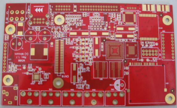
Impedance PCB board introduction
Impedance PCB board refers to the PCB board that needs impedance control. Impedance control means that under a high-frequency signal, the "resistance" generated by a certain circuit layer to its reference layer during transmission must be controlled within the rated range to ensure that the signal is not distorted during transmission. Impedance control is actually to make every part of the system have the same impedance value, that is, impedance matching.

Impedance PCB board function
1. In the production process, the PCB board has to go through process steps such as copper sinking, electroplating tin, and connector soldering, and the materials used in these links must ensure the low resistivity to ensure that the overall impedance of the circuit board is low to meet the product quality requirements. Can operate normally.
2, tin plating is the most prone to problems in the entire circuit board production, and it is a key link that affects impedance. The biggest drawbacks are easy discoloration (both easy to oxidize or deliquesce), poor solderability, which can lead to difficult soldering of circuit boards, high impedance, poor electrical conductivity, or instability of overall board performance.
3. There will be various signal transmissions in the conductors in the circuit board. When the frequency must be increased to increase its transmission rate, the circuit itself will change the impedance value due to factors such as etching, laminate thickness, and wire width. Distorting its signal, resulting in a decrease in the performance of the circuit board, so it is necessary to control the impedance value within a certain range.
4. In the process, we should consider installing the components. After plugging, we should consider the electrical performance and signal transmission issues. Therefore, at this time, the lower the impedance, the better.
What is false copper exposure
After the PCB circuit is etched, a layer of ink (green oil, blue oil, black oil, etc.) needs to be brushed. The ink is liquid and has fluidity. During the curing process after brushing, there will be an uneven state of the ink, mainly In this case, some positions are detected with a magnifying glass, and there is a suspected ink not being brushed. If the copper surface is exposed, it is a false exposure of copper.

Reasons for false copper exposure:
1. In the solder mask process, when the mantissa clearing board is produced, the plug hole net is not used for production, and the empty net is used for continuous printing with plugging. The plug hole is not full, and the ink shrinks after the post-baking, which causes false edge of the hole. Exposed copper.
2. The ink in the hole of the heavy-duty board hole of the welding mask is not cleaned, causing the ink to be unable to plug through the hole during the second printing, and the plug hole is not full, causing false copper exposure.
3. When printing plug holes in the current operation mode, the first side is directly on the printing press table. Because the table is flat, it is not convenient for air to escape from the holes, which leads to incomplete plugging of some holes, causing false copper exposure.
4. Missing personnel inspection.
Those that have an impact on the function of the board can be sent directly to the factory for re-opening and production. Do not try to use it because once it is used, the loss caused by a problem is not the loss of a board, but more of the loss is the components on the circuit board. Avoid loss. If the copper leakage is visible to the naked eye, send it directly to the original board factory.