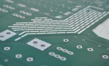
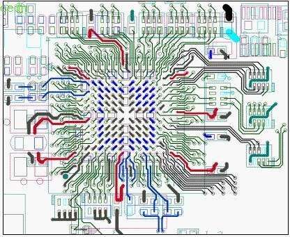
HDI is a kind of PCB board product, the full name is highDensityInterconnection, high-density interconnection board At present, high-end electronic products are generally HDI board products.
Blind vias: Blind vias are vias that connect the traces on the inner layer of the PCB to the traces on the surface of the PCB. This hole does not penetrate the entire board.
Buried vias: Buried vias are the type of vias that only connect the traces between the inner layers, so they are invisible from the surface of the PCB.

With the development of the current portable product design in the direction of miniaturization and high density, PCB design is becoming more and more difficult, and higher requirements are placed on the PCB production process. In most of the current portable products, the BGA package with a pitch of less than 0.65mm uses the design process of blind and buried vias. So what is the blind and buried via?
Blind vias: Blind vias are vias that connect the inner traces of the PCB with the traces on the surface of the circuit board. This hole does not penetrate the entire board.
Buried vias: Buried vias are the type of vias that only connect the traces between the inner layers, so they are invisible from the surface of the PCB.
PCB boards with buried blind vias are not necessarily HDI circuit boards, but generally HDI boards have blind vias, but buried vias are not necessarily the case. It depends on how many orders and pressures your circuit board product is.
Blind Buried Hole Plate
described as follows:
The first order and the second order of the 6-layer circuit board are for the board that needs laser drilling, that is, the HDI board.
The first-order HDI board of 6-layer circuit board refers to blind holes: 1-2, 2-5, 5-6. That is, 1-2, 5-6 need laser drilling.
The 6-layer circuit board second-order HDI board refers to blind holes: 1-2, 2-3, 3-4, 4-5, 5-6. That is, 2 laser drilling is required.
First drill 3-4 buried holes, then press 2-5, then drill 2-3, 4-5 laser holes for the first time, then press 1-6 for the second time, then drill 1-2 for the second time, 5-6 laser holes. Finally, the through holes are drilled. It can be seen that the second-order HDI board has been pressed twice and laser drilled twice.
In addition, second-order HDI boards are also divided into: second-order HDI boards with wrong holes and second-order HDI boards with stacked holes. Board refers to the blind holes 1-2 and 2-3 stacked together, for example: blind: 1-3, 3-4, 4-6.
And so on, third-order, fourth-order... are all the same.
In PCB design, avoid using a single large pad between two interconnected SMD components, because the solder on the large pad will pull the two components to the middle. The correct way is to solder the two components. Separate the disks and connect them with a thinner wire between the two pads. If the wires are required to pass a larger current, several wires can be connected in parallel;
During PCB design, there should be no through holes on or near the pads of the parts. Otherwise, during the process, the solder on the pads will flow along the through holes after melting, resulting in false soldering, less tin, or flow to the board. The other side causes a short circuit; the types of pin spacing (ie pad spacing) between the axial device and the jumper should be minimized to reduce the number of adjustments of device molding and improve the efficiency of the plug-in;

Solder resist should be added between the pads of the chip ICs that need wave soldering, and the tin-stealing pads should be designed on the last leg;
When the PCB design does not make special requirements, the component hole shape, the shape of the pad and the component foot must match, and the symmetry of the pad relative to the hole center should be ensured (square component foot formula-shaped component hole, square pad; round component foot configuration Circular component holes, circular pads) to ensure that the solder joints are full of tin;
For components that need to be soldered after going through the tin furnace, the soldering pad should be driven away from the tin position, and the direction is opposite to the tin passing direction, and the width of the hole is 0.5~1.0mm to prevent the hole from being blocked after the wave crest;
Increase the copper skin and increase the gravitational force of the side pins to facilitate self-centering of reflow soldering.