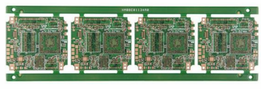
Sequential lamination method The generation and technical requirements of buried/blind vias:
From the beginning of the 20th century to the beginning of the 21st century, the development of electronic housing technology has advanced by leaps and bounds, and the electronic assembly technology has rapidly improved. As the printed circuit board industry, only by developing in sync with it, can it meet the needs of customers. With the small, light and thin electronic products, printed circuit boards have developed flexible boards, rigid-flex boards, buried/blind-hole multilayer PCB boards, and so on. However, the investment in printed circuit board production equipment is quite large, especially the equipment for making multi-layer PCB boards with in/blind holes, such as laser drilling machines, pulse plating equipment, etc. For ordinary small and medium-sized enterprises, especially those enterprises that do not mass produce buried/blind-via multilayer PCB boards, it is impossible to invest so much capital to purchase equipment. Therefore, the use of existing equipment to produce buried/blind-via multilayer PCB boards has a certain value. This not only expands the company's product categories, but also meets the needs of some customers. This article always discusses some of the encounters in this production process.

1 CAD wiring
Using the traditional lamination method and then according to the needs of the lamination, the method of laminating in stages, we call this process the sequential lamination method. It can be seen that this method has certain technological limitations, that is, it cannot be arbitrarily interconnected. So, we must clarify this limitation when we carry out CAD wiring. First, it is recommended to use more buried vias; second, use less blind vias. If blind vias are used, the interconnection should not exceed half of the total number of layers. This can reduce the number of laminations and the difficulty of processing.
2 Inner layer production
When producing multi-layer PCB boards with buried/blind holes, some of the inner layer boards have metallized holes, and some may not have metallized holes, so they must be marked and distinguished during production; the file of the inner layer drilling program The name corresponds to the logo of the inner core board, and it must be clearly stated in the process documents; the anti-corrosion of the inner board can be masked by dry film or pattern electroplating, depending on the habits of different manufacturers and the The proficiency of the process.
3 laminated
When the inner layer board is processed, and then blackened or browned, it can be pre-stacked and laminated. This process should pay attention to the following aspects; first, whether the laminating sequence is correct; second, whether the inner layer is correct during lamination; third, whether the amount of resin in the interlayer prepreg is sufficient, and whether the holes can be filled. When drafting the production specifications, it is necessary to choose the semi-cured model and quantity; finally, pay attention to whether the choice of copper foil thickness is reasonable, because when blindly making, the patterns on both sides are not formed at the same time, and the plating time is also different.
4 Outer layer graphics production
There is no essential difference between the outer layer graphics production and ordinary double-sided, multi-layer PCB boards. It is worth noting that due to the existence of blind holes, the copper foil thickness of the top and bottom layers is not necessarily the same. There is a certain degree of difficulty in etching. Appropriate compensation should be made when light drawing the film. On the other hand, due to the different thickness of the copper foil, the stress There are also differences. The warpage of the finished board is most likely to occur. When there are more levels of interconnected blind holes, the warpage is more obvious. Therefore, you can consider using core boards of different thicknesses in the stack design to eliminate this part. Stress to avoid warping of the finished board.