With the increase in the number of layers of printed circuit boards, the production cost will increase sharply, so it is possible that the cost may vary greatly due to the difference of ideas. If you encounter difficulties in designing a 6-layer printed circuit board, you must not give up lightly. Perhaps the large amount of economic benefits lies in your persistent efforts; however, it is not easy to make it difficult, because when When encountering this kind of thing, the designer may choose to design an 8-layer printed circuit without hesitation in most cases.
With the increase in the number of layers of printed circuit boards, the production cost will increase sharply, so it is possible that the cost may vary greatly due to the difference of ideas. If you encounter difficulties in designing a 6-layer printed circuit board, you must not give up lightly. Perhaps the large amount of economic benefits lies in your persistent efforts; however, it is not easy to make it difficult, because when When encountering this kind of thing, the designer may choose to design an 8-layer printed circuit without hesitation in most cases.
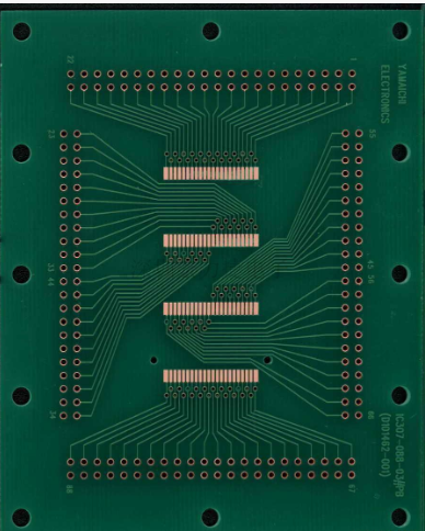
If the width of the conductive pattern in the printed circuit board is represented by L and the width of the gap between the conductor patterns is represented by S, then LIS represents the ratio of the width of the conductive strip to the width of the gap. As this ratio decreases, the production yield of printed circuit boards will drastically decrease, and the cost will also rise. This phenomenon is more obvious when the circuit density is relatively high. Therefore, the value of LIS must not be arbitrarily reduced.

In the case of using a drill bit to perforate the printed circuit board, when the hole diameter is lower than a certain value, the drilling depth of a drill bit will be shortened sharply. That is to say, when drilling a hole with a small diameter, the drill needs to withdraw the heat for many times, which will reduce the production efficiency and increase the cost. Therefore, do not arbitrarily reduce the aperture of the through holes; moreover, the number of through holes should be reduced as much as possible.
For the through holes of the double-sided PCB circuit board, the method of copper plating is not used to realize the connection of the two-sided circuits, but the method of filling the through holes with silver paste can also reduce the cost of the double-sided printed circuit board. This method is generally used for ordinary phenolic resin paperboard with copper-clad on both sides. This method first cleans the surface of ordinary phenolic resin paperboard coated with copper on both sides, and then prints a resist pattern on both sides by screen printing. After etching, a conductor pattern is formed. After removing the resist layer, a through hole is punched. Fill the hole with silver paste. In order to make the silver paste have good contact with the conductor patterns on both sides, the silver paste should bulge through the through holes, and the diameter of the silver paste pattern at the bulging part is larger than the hole diameter of the through holes. In order to prevent the migration of silver ions, a covering layer was applied on the surface of the bulging part of the silver paste by screen printing. Then, the solder mask pattern and isolation pattern are screen printed on both sides, and the screw holes for fixing the printed circuit board are punched or drilled to process the shape. Finally, through inspection, the double-sided printed circuit board with silver paste filled through holes was completed.
Generally speaking, due to the base material, this silver paste filled through-hole double-sided printed circuit board is not suitable for high-reliability circuits. In addition, since the silver paste contains a large number of non-conductive materials in addition to conductive substances, the conductivity of silver paste is not as good as that of copper foil, and readers should also be reminded.
Strict control of the quantity of materials can achieve energy saving and emission reduction in the manufacturing process, and meet the requirements of green production while reducing cost input. Mainly reflected in the following points: The printed board is a non-universal (or characteristic) commodity. If there is too much production, customers will reject and waste, and if there is less production, we need to re-feed materials, resulting in waste of materials, labor, water and electricity, and time. How to reasonably control the quantity of feeding materials? One is that it depends on the control scope of the customer's real demand and requires the salesperson to ask the customer clearly. Second, it depends on the control ability of the production and processing process, evaluates and calculates, optimizes the quantity of materials; strengthens the control of the remaining number of finished boards. According to customers, product models, and remaining quantities, carry out inventory and accounting, and convey the remaining information to customers, engineering, production, and planning personnel. Make full use of the remaining inventory PCB printed boards, digest or reduce the inventory of finished boards, reduce the amount of finished boards, and control rework/replenishment. It is necessary to investigate the reasons and responsibilities of rework/scrap, implement financial penalties, and correct the violation of operations or failure to perform duties.