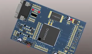
The following are the common problems and improvement methods of resin plug holes in the PCB manufacturing process of PCB factories.
1 For POFV products
1.1 Common problems
A. Orifice bubbles
B. The plug hole is not full
C, resin and copper layering
1.2 Consequences
A. There is no way to make pads on the orifice; the orifice contains gas, and the chip mount blowing is also called out-gassing.
B. No copper in the hole
C. PCB pads protrude, causing components not to be attached or components to fall off
1.3 Preventive improvement measures
A. Choose appropriate plugging ink, control the storage conditions and shelf life of the ink,
B. Standard inspection process to avoid the appearance of holes in the patch position. Even if you can rely on the excellent plug hole

technology and good silk screen conditions to improve the yield of the plug hole, the probability of one in ten thousand can also cause the product to be scrapped. Sometimes it is really scrapped because of a hole in the hole and there is no pad on the hole. pity. This can only be done through inspection to find the location of the cavity and repair it. Of course, the problem of checking the voids of resin plug holes has always been discussed, but it seems that there is no good equipment that can solve this problem. There are many different ways to make the accuracy of manual inspection and judgment higher.
C. Choose the right resin, especially the choice of material Tg and expansion coefficient, the right production process and the right degumming parameters, to avoid the problem of the pad and the resin being separated after heating.
D. Regarding the problem of resin and copper delamination, we found that when the thickness of the copper on the surface of the hole is greater than 15um, the problem of such resin and copper delamination can be greatly improved.
2 PCB inner layer HDI buried hole, blind hole plug hole resin plug hole
2.1 Common problems
A, burst board
B. Blind hole resin protrusions
C, hole without copper
2.2 Consequences
Needless to say, the above several problems directly lead to the scrap of the product. The protrusions of the resin often cause uneven lines and lead to open and short circuits.
2.3 Preventive improvement measures
A. Controlling the fullness of the HDI plug holes in the PCB inner layer is a necessary condition to prevent board explosion; if you choose to plug the holes after the circuit, you must control the time between the plug holes and the pressing and the cleanliness of the board surface.
B. The protrusion control of the resin needs to control the grinding and flattening of the resin;
3. Promotion of resin plugging technology
With the continuous improvement of the proficiency in the application of resin plugging technology and the effective solution of stubborn problems such as bubbles, the resin plugging technology is continuously being promoted. For example, HDI blind holes are filled with resin, and the inner layer HDI buried hole VIP process of laminated HDI structure and so on.
In the current standard (IPC-650) in the PCB industry, it seems that there is no requirement for the copper thickness on the hole of the resin plug hole. The potential risk is that once the thickness of the copper plated on the hole of the resin plug hole is too thin, After the surface treatment of the inner HDI circuit and the browning treatment, the thin copper on the hole may be drilled through by laser drilling, and it cannot be judged as a problem in the electrical test. But the quality of this thin layer of copper in terms of high pressure resistance is really worrying.
On this issue, according to our experimental data, if the copper thickness above the buried hole can be guaranteed to be greater than 15um, which meets Hoz's completed copper thickness requirements, there will generally be no abnormal quality. Of course, if the customer has higher continuity requirements, it is another matter.
in conclusion
After years of development, the technology of resin plugging has been gradually accepted by many users, and continues to play its indispensable role in some high-end products. Especially in blind buried vias, HDI, thick copper and other products have been widely used, these products involve communications, military, aviation, power, network and other industries. As a manufacturer of PCB products, we understand the process characteristics and application methods of resin plugging technology. We also need to continuously improve the process capability of resin plugging products, improve product quality, and solve the related process problems of such products. Good and promote this kind of technology to realize the production of higher technical difficulty PCB products.