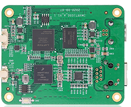
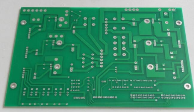
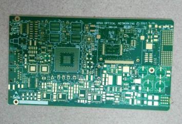
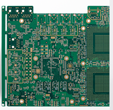
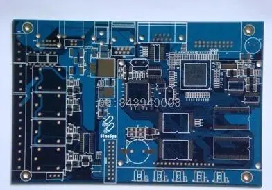
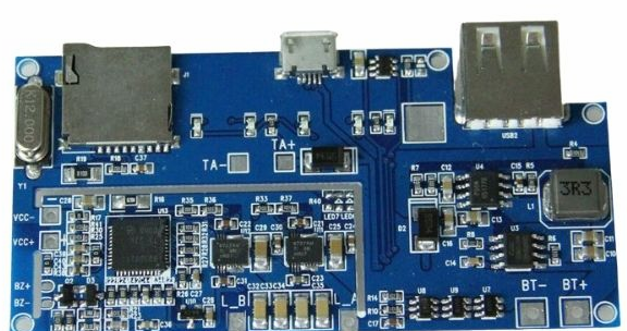
In the process of PCB board production, there are many processes. I have sorted out how to regulate these process requirements in the process of PCB board production, and what are the design and production process standards for PCB board production.
a) The layout of printed wires and pads? The line width and line spacing are in principle specified in the design drawings. However, our company will perform the following processing: According to the process requirements, the line width? PAD ring width will be compensated. For single panel, we will increase PAD as much as possible to improve the reliability of customer welding
b) When the design line spacing does not meet the process requirements (too dense may affect the performance? Manufacturability), we will adjust according to the pre-design specifications.
c) In principle, some PCB companies suggest that when designing single and double panels, the through hole inner diameter (VIA) is set to be 0.3mm or more, the outer diameter is set to be 0.7mm or more, the line spacing is designed to be 8mil, and the line width is designed to be 8mil or greater. Minimize the production cycle and reduce the difficulty of manufacturing.
d) Our smallest drilling tool is 0.3, and the finished hole is about 0.15mm. The minimum line spacing is 6 mils. The thinnest line width is 6 mils. (But the manufacturing cycle is longer, which is? The cost is higher)

2. Line width tolerance
Internal control standard for printing line width tolerance is ±15%
3. Grid processing
a) In order to avoid polishing of the copper surface during the wave soldering process and PCB bending due to thermal stress after heating, it is recommended to lay the large copper surface in a grid form.
b) Grid spacing ≥ 10 mils (not less than 8 mils), and grid line width ≥ 10 mils (not less than 8 mils).
4. Thermal pad treatment
In large-area grounding (electricity), the legs of the components are usually connected to them. The operation of the connecting legs takes into account electrical performance and process requirements, and a cross-shaped pad (insulating pad) can be used to form a cross section during soldering. The possibility of excessively dispersing heat to produce virtual solder joints is greatly reduced.
Five apertures (HOLE)
1. Metallization (PHT) and non-metallization (NPTH)
a) Our default value is as follows: non-metallized hole:
When the customer sets the non-metallized properties of the mounting holes in the advanced properties of Protel99se (the plating item is deleted from the advanced menu), our default value is non-metallized holes.
When the customer directly uses the holding layer or the mechanical 1-layer arc to indicate the hole in the design file (there is no separate hole), our default value is the non-metalized hole.
When the customer puts the NPTH word near the hole, we default that the hole is non-metallized.
When the customer clearly requires the corresponding pore non-metallization (NPTH) in the design notice, we will deal with it according to the customer's requirements. b) Component holes, mounting holes, and through holes other than the above should be metallized.
2 Aperture size and tolerance
a) The PCB component hole in the design pattern? The mounting hole defaults to the final finished hole size. The aperture tolerance is generally ±3mil (0.08mm);
b) Through hole (ie VIA hole) our general control is: no negative tolerance is required, and the positive tolerance is controlled within + 3mil (0.08mm).
3 thickness
The average thickness of the copper plating of the metallized holes is usually not less than 20μm, and the thinnest part is not less than 18μm.
4 Hole wall roughness
PTH hole wall roughness is generally controlled within ≤32um
5 Pinhole problem
a) The positioning pin of our CNC milling machine is at least 0.9mm, and the three PIN holes for positioning should be triangular.
b) When the customer has no special requirements, and the aperture of the design document is <0.9mm, some PCB companies will add PIN holes in the appropriate positions on the blank wireless road or the large copper surface of the board.