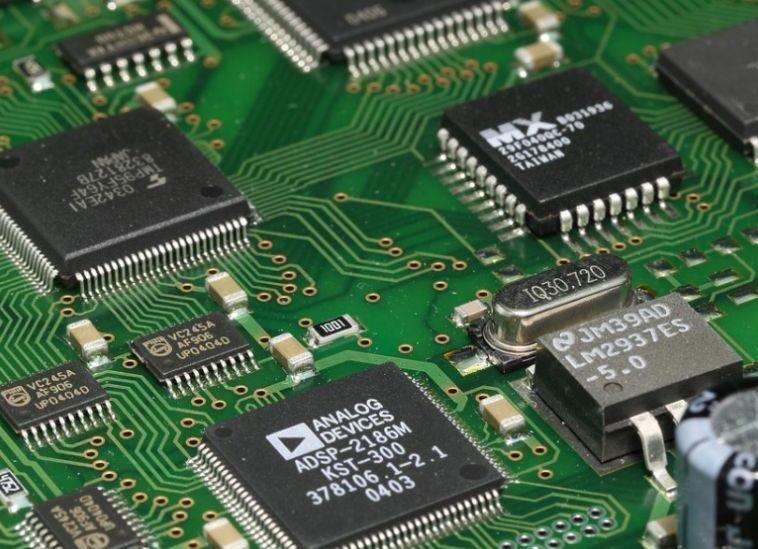
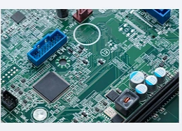
The vias of the PCB copy board appear as discontinuous breakpoints on the transmission line, which will cause signal reflection. Generally, the equivalent impedance of the via is about 12% lower than that of the transmission line. For example, the impedance of a 50 ohm transmission line will decrease by 6 ohms when passing through the via (specifically, it is related to the size and thickness of the via, not an absolute reduction). However, the reflection caused by the discontinuous impedance of the via is actually very small. The reflection coefficient is only: (44-50)/(44+50)=0.06. The problems caused by the via are more concentrated on the parasitic capacitance and inductance. Impact.
The via itself has parasitic stray capacitance. If it is known that the diameter of the solder mask on the ground layer of the via is D2, the diameter of the via pad is D1, the thickness of the PCB board is T, and the dielectric constant of the board substrate For ε,

the parasitic capacitance of the via is similar to: C=1.41ε The parasitic capacitance of the via will have the main effect on the circuit is to prolong the rise time of the signal and reduce the speed of the circuit. For example, for a PCB with a thickness of 50Mil, if the diameter of the via pad is 20Mil (the diameter of the hole is 10Mils), and the diameter of the solder mask is 40Mil, then we can approximate the through hole by the above formula The parasitic capacitance is roughly:
The rise time change caused by this part of the capacitance is roughly:
From these values, it can be seen that although the effect of the rise delay caused by the parasitic capacitance of a single via is not very obvious, if the via is used multiple times in the trace to switch between layers, multiple vias will be used., The design must be carefully considered. In the actual design, the parasitic capacitance can be reduced by increasing the distance between the via and the copper area (Anti-pad) or reducing the diameter of the pad.
There are parasitic capacitances in vias and parasitic inductances. In the design of high-speed digital PCB circuits, the damage caused by the parasitic inductances of vias is often greater than the impact of parasitic capacitance. Its parasitic series inductance will weaken the contribution of the bypass capacitor and weaken the filtering effect of the entire power system. We can use the following empirical formula to simply calculate the parasitic inductance of a via:
where L refers to the inductance of the via, h is the length of the via, and d is the diameter of the center hole. It can be seen from the formula that the diameter of the via has a small influence on the inductance, and the length of the via has the greatest influence on the inductance. Still using the above example, the inductance of the via can be calculated as:
If the rise time of the signal is 1ns, then the equivalent impedance is: XL=πL/T10-90=3.19Ω. Such impedance can no longer be ignored when high-frequency currents pass. Special attention should be paid to the fact that the bypass capacitor needs to pass through two vias when connecting the power plane and the ground plane, so that the parasitic inductance of the vias will increase exponentially.
Through the above analysis of the parasitic characteristics of vias, it can be seen that in high-speed PCB design, seemingly simple vias will often bring great negative effects to the circuit design. In order to reduce the adverse effects caused by the parasitic effects of vias, the following can be done in the design:
·From cost and signal quality considerations, choose a reasonable size via size. If necessary, you can consider using different sizes of vias. For example, for power or ground vias, you can consider using a larger size to reduce impedance, and for signal traces, you can use smaller vias. Of course, as the size of the via decreases, the corresponding cost will increase.
·The two formulas discussed above can be concluded that the use of a thinner PCB is beneficial to reduce the two parasitic parameters of the via.
·The signal traces on the PCB board should not be changed as much as possible, which means that unnecessary vias should not be used as much as possible.
·The pins of the power supply and the ground should be drilled nearby, and the lead between the via and the pin should be as short as possible. Consider playing multiple vias in parallel to reduce the equivalent inductance.