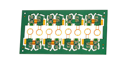
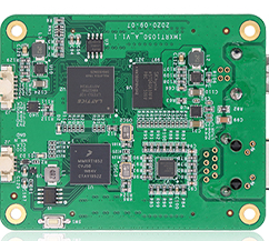
Do you know "Why the PCB must be baked after the expiration date exceeds the shelf life before the SMT can be used in the reflow oven"?
The main purpose of PCB baking is to dehumidify and remove moisture, and to remove the moisture contained in the PCB or absorbed from the outside, because some materials used in the PCB itself are easy to form water molecules.
In addition, after the PCB is produced and placed for a period of time, there is a chance to absorb moisture in the environment, and water is one of the main killers of PCB popcorn or delamination. Because when the PCB is placed in an environment where the temperature exceeds 100°C, such as reflow oven, wave soldering oven, hot air leveling or hand soldering, the water will turn into water vapor and then rapidly expand its volume.
The faster the heating speed of the PCB, the faster the expansion of water vapor; the higher the temperature, the larger the volume of water vapor; when the water vapor cannot escape from the PCB immediately, there is a good chance of expanding the PCB .
In particular, the Z direction of the PCB is the most fragile. Sometimes the vias between the layers of the PCB may be broken, and sometimes it may cause the separation of the layers of the PCB. More seriously, even the appearance of the PCB can be seen. Phenomenon such as blistering, swelling, bursting, etc.;

Sometimes even if the above phenomena are not visible on the outside of the PCB, it is actually internally injured. Over time, it will cause unstable functions of electrical products, or CAF and other problems, which will eventually cause the product to fail.
Analysis of the true cause of PCB explosion and preventive countermeasures
The PCB baking procedure is actually quite troublesome. During baking, the original packaging must be removed before it can be put in the oven, and then the temperature must be over 100 degree Celsius for baking, but the temperature should not be too high to avoid the baking period. Excessive expansion of water vapor actually bursts the PCB.
Generally, the PCB baking temperature is generally set at 120±5 degree Celsius in the industry to ensure that moisture can really be eliminated from the PCB body before the SMT line can be used for reflow soldering.
The baking time varies with the thickness and size of the PCB. For thinner or larger PCBs, you have to press the board with a heavy object after baking. This is to reduce or avoid the PCB The tragic occurrence of PCB bending deformation due to stress release during cooling after baking.
Because once the PCB is deformed and bent, there will be problems of offset or uneven thickness when printing the solder paste in SMT, which will cause a large number of solder short circuits or empty soldering defects during the subsequent reflow.
PCB baking condition setting
At present, the industry generally sets the conditions and time for PCB baking as follows:
1. The PCB is well sealed within 2 months of the manufacturing date. After unpacking, it is placed in a temperature and humidity controlled environment (≦30 degree Celsius/60%RH, according to IPC-1601) for more than 5 days. Bake at 120±5 degree Celsius for 1 hour.
2. The PCB is stored for 2 to 6 months beyond the manufacturing date, and it must be baked at 120±5°C for 2 hours before going online.
3. The PCB is stored for 6-12 months beyond the manufacturing date, and it must be baked at 120±5°C for 4 hours before going online.
4. PCB is stored for more than 12 months from the manufacturing date, basically it is not recommended, because the adhesive force of the multilayer board will age over time, and quality problems such as unstable product functions may occur in the future, which will increase the market for repairs. In addition, there are risks of plate bursting and poor tin eating during the production process. If it is not allowed to be used, it is recommended to bake at 120±5 degree Celsius for 6 hours. Before mass production, first try to print a few pieces of solder paste and make sure that there is no solderability problem before continuing production.
Another reason is that it is not recommended to use PCBs that have been stored for too long because their surface treatment will gradually fail over time. For ENIG, the industry’s shelf life is 12 months. The thickness depends on the thickness. If the thickness is thinner, the nickel layer may appear on the gold layer due to the diffusion effect and form oxidation, which will affect the reliability, so you should not be careful.
5. All PCBs that have been baked must be used within 5 days, and unprocessed PCBs must be baked at 120±5°C for another 1 hour before going online.
Stacking method during PCB baking
1. When baking large-size PCBs, use a horizontal stacking arrangement. It is recommended that the maximum number of a stack should not exceed 30 pieces. The oven needs to be opened within 10 minutes after the baking is completed to take out the PCB and lay it flat to cool it. Press after baking Anti-bend fixtures. Large-size PCBs are not recommended for vertical baking, as they are easy to bend.
2. When small and medium-sized PCBs are baked, they can be placed horizontally and stacked. The maximum number of a stack should not exceed 40 pieces, or it can be upright, and the number is not limited. You need to open the oven and take out the PCB within 10 minutes after the baking is completed. Allow it to cool, and press the anti-bending jig after baking.
Precautions when PCB baking
1. The baking temperature should not exceed the Tg point of the PCB, and the general requirement should not exceed 125°C. In the early days, the Tg point of some lead-containing PCBs was relatively low, and now the Tg of lead-free PCBs is mostly above 150°C.
2. The baked PCB should be used up as soon as possible. If it is not used up, it should be vacuum packed as soon as possible. If exposed to the workshop for too long, it must be baked again.
3. Remember to install ventilation drying equipment in the oven, otherwise the steam will stay in the oven and increase its relative humidity, which will not dehumidify the PCB.
4. From a quality point of view, the more fresh the PCB solder is used, the better the quality after the oven. The expired PCB will still have a certain quality risk even if it is used after baking.
Recommendations for PCB baking
1. It is recommended to use a temperature of 105±5 degree Celsius to bake the PCB, because the boiling point of water is 100 degree Celsius, as long as it exceeds its boiling point, the water will become steam. Because PCB does not contain too many water molecules, it does not require too high a temperature to increase the rate of its vaporization.
If the temperature is too high or the gasification rate is too fast, it will easily cause the water vapor to expand quickly, which is actually bad for the quality, especially for multilayer boards and PCBs with buried holes. 105 degree Celsius is just above the boiling point of water, and the temperature will not be too high., Can dehumidify and reduce the risk of oxidation. Moreover, the ability of the current oven to control the temperature has been improved a lot.
2. Whether the PCB needs to be baked depends on whether its packaging is damp, that is, to observe whether the HIC (Humidity Indicator Card) in the vacuum packaging has shown that it has been damp. If the packaging is good, HIC does not indicate that the dampness is actually It can be put directly on the line without baking.
3. It is recommended to use "upright" and spaced baking when PCB baking, because this can achieve the maximum effect of hot air convection, and moisture is easier to be baked out of the PCB. However, for large-size PCBs, it may be necessary to consider whether the vertical type will cause bending and deformation of the board.
4. After the PCB is baked, it is recommended to place it in a dry place and allow it to cool quickly. It is better to press the "anti-bending jig" on the top of the board, because the general object is easy to absorb water vapor from the high heat state to the cooling process. However, rapid cooling may cause plate bending, which requires a balance.
Disadvantages of PCB baking and things to consider
1. Baking will accelerate the oxidation of the PCB surface coating, and the higher the temperature, the longer the baking, the more unfavorable.
2. It is not recommended to bake OSP surface-treated boards at a high temperature, because the OSP film will degrade or fail due to high temperature. If you have to bake, it is recommended to bake at a temperature of 105±5°C, not more than 2 hours, and it is recommended to use it up within 24 hours after baking.
3. Baking may have an impact on the formation of IMC, especially for HASL (tin spray), ImSn (chemical tin, immersion tin plating) surface treatment boards, because the IMC layer (copper tin compound) is actually as early as the PCB stage Generation, that is, it has been generated before PCB soldering, and baking will increase the thickness of this layer of IMC that has been generated, causing reliability problems.