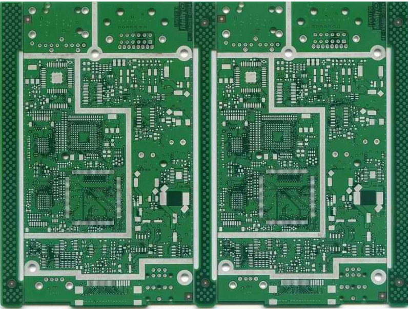
In the design and manufacturing process of high-speed PCB printed circuit boards, engineers need to start with wiring and component settings to ensure that this PCB board has good signal transmission integrity. In today's article, we will introduce some wiring techniques that are often used in PCB signal integrity design for newcomers engineers, hoping to bring some help to newcomers' daily study and work.
PCB printed circuit board wiring
In the design process of high-speed PCB printed circuit boards, the cost of the printed circuit of the substrate is proportional to the number of layers and the surface area of the substrate. Therefore, under the premise of not affecting the system function and stability, engineers should use the least number of layers to meet the actual design needs, which will inevitably increase the wiring density. In the PCB wiring design, the greater the wiring width Fine, the smaller the interval, the greater the crosstalk between signals, and the smaller the transmission power. Therefore, the selection of trace size must consider various factors.
In the PCB layout design process, the principles that engineers need to follow are mainly as follows:
First of all, designers should minimize the bending of the leads between the pins of high-speed circuit devices during the wiring process, and use 45-degree folding lines to reduce external reflection and mutual coupling of high-frequency signals.
Secondly, when performing the wiring operation of the PCB board, the designer should shorten the lead between the pins of the high-frequency circuit device as much as possible and the inter-layer alternation of the lead between the pins. High-frequency digital signal traces should be as far away as possible from analog circuits and control circuits.
In addition to the precautions for PCB wiring mentioned above, engineers also need to be cautious when dealing with differential signals. Because the differential signal has the same amplitude and the same direction, the magnetic fields generated by the two signal lines cancel each other out, which can effectively reduce EMI. The spacing of the differential lines often leads to changes in the differential impedance, and the inconsistency of the differential impedance will seriously affect the signal integrity. Therefore, in actual differential wiring, the difference in length between the two signal lines of the differential signal must be controlled at the time of the rising edge of the signal. Within 20% of the electrical length. If conditions permit, the differential wiring must meet the back-to-back principle and be in the same wiring layer. In the setting of the line spacing of differential wiring, engineers need to ensure that it is at least equal to or greater than 1 times the line width. The distance between differential traces and other signal lines should be greater than three times the line width.

Shielding methods in high-speed PCB design
The transmission rate of high-speed PCB design and wiring systems is steadily accelerating, but it also brings a certain anti-interference vulnerability. This is because the higher the frequency of transmission of information, the increase in signal sensitivity, and their energy is getting weaker and weaker. At this time, the wiring system is more susceptible to interference.
High-speed PCB layout design
Interference is everywhere. Cables and equipment will interfere with other components or be seriously interfered by other sources of interference, such as: computer screens, mobile phones, electric motors, radio relay equipment, data transmission and power cables, etc. In addition, potential eavesdroppers, cybercrime, and hackers are increasing because their interception of UTP cable information transmission will cause huge damages and losses.
Especially when using a high-speed data network, the time required to intercept a large amount of information is significantly lower than the time required to intercept low-speed data transmission. The twisted pair in the data twisted pair can rely on its own twisting to resist external interference and crosstalk between the pairs at low frequencies, but at high frequencies (especially when the frequency exceeds 250MHz), only rely on Wire pair twisting can no longer achieve the purpose of anti-interference, and only shielding can resist external interference.
The function of the cable shielding layer is like a Faraday shield, interference signals will enter the shielding layer, but not into the conductor. Therefore, the data transmission can run without failure. Since shielded cables have lower radiation emission than unshielded cables, the network transmission is prevented from being intercepted. The shielded network (shielded cables and components) can significantly reduce the electromagnetic energy radiation level that may be intercepted when entering the surrounding environment.
Shielding selection of different interference fields There are two main types of interference fields: electromagnetic interference and radio frequency interference. Electromagnetic interference (EMI) is mainly low-frequency interference. Motors, fluorescent lights, and power lines are common sources of electromagnetic interference. Radio frequency interference (RFI) refers to radio frequency interference, mainly high frequency interference. Radio, television broadcasting, radar and other wireless communications are common sources of radio frequency interference.
For resistance to electromagnetic interference, the choice of braided shield is the most effective because it has a lower critical resistance; for radio frequency interference, the foil shield is the most effective, because the braided shield depends on the change of wavelength, and the gap it produces makes high-frequency signals free In and out of the conductor; and for the mixed interference field of high and low frequency, the combined shielding method of foil layer and woven net with broadband coverage function should be adopted. Generally, the higher the mesh shielding coverage, the better the shielding effect.