After helping customers make their products comply with EMI standards, a potential problem was discovered: poor PC board design. Based on experience, designers of IoT products have encountered problems caused by poor PC board design. When onboard energy destroys sensitive receiver circuits, poor design can cause infinite delays, which can lead to cellular compliance failures. GPS and Wi-Fi receivers will also lose sensitivity.
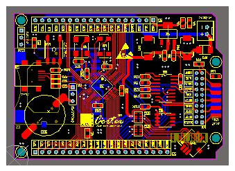
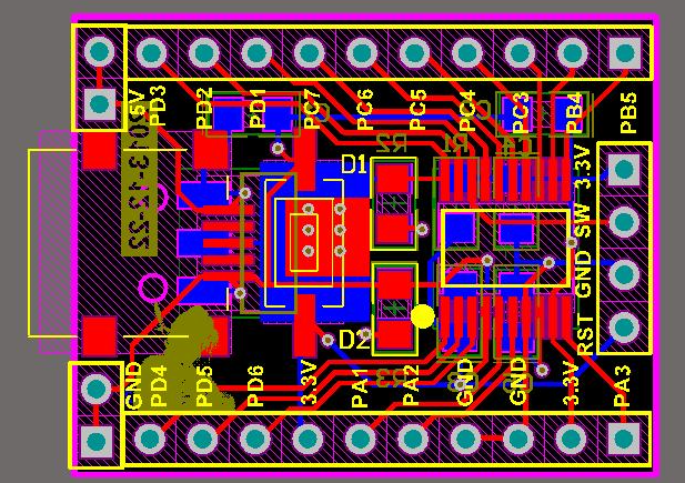
How the signal travels through the PCB and how the electromagnetic field moves affect that movement. The difference between good and bad PCB stackup.
There are many factors that contribute to poor EMI design. These include:
Use digital and sensitive analog circuits to mix noise circuits, such as power supply and motor conversion.
Place the clock driver too close to the edge of the circuit board or close to sensitive circuits.
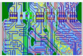
Poor routing that causes crosstalk.
Run clock (or high-speed) traces on the gaps/slots of the return plane.
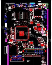
Most importantly, the wrong layer stacking.
The crossover clock traces on the return plane gap have been resolved. However, fixing the last item about layer overlays usually corrects countless drawbacks, including many other items on the list.

When attending college circuit courses, most of us were mistakenly taught how DC and AC current work in lumped or distributed (transmission line) circuits. In our "Fields and Waves" course, we are unlikely to be instructed in the practical application of circuit board design or the propagation of signals through the circuit board. In fact, these two concepts-circuits and fields-work together (complementary) when propagating a digital signal through a microstrip line or stripline.
Before you can understand how the signal propagates in the PC board, you must first understand some physics.
We are all taught that the "current" is the flowing copper of electrons. This is close to the truth, except that we tend to think about positive currents-lack of electrons, often called "holes". However, electrons and the "holes" (positive charges) they leave behind travel very slowly.
Of course, this current is correct for the DC circuit (except for the initial battery connection transient). But for the "DC" output (with transients) of AC (or radio frequency) circuits or switch-mode power supplies, we need to understand that all connection lines/wiring must now consider transmission lines.
Results First, let us consider how the capacitor seems to allow electrons to flow. After all, isn't this the working principle of decoupling capacitors? If we apply a battery to a capacitor, any positive charge applied to the top plate will repel the positive charge on the bottom plate, leaving a negative charge. If we apply AC power to capacitors, you might think that current flows through the dielectric, which is impossible. James Clerk Maxwell called it "displacement current", where the positive charge only replaces the positive charge on the opposite plate and leaves the negative charge, and vice versa. This displacement current is defined as dE / dt (time-varying electric field).