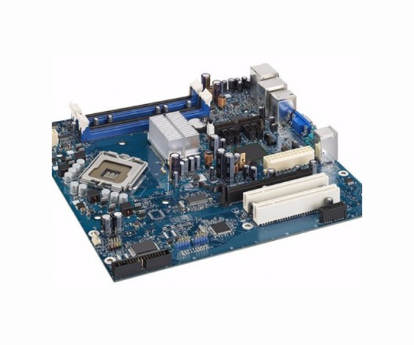
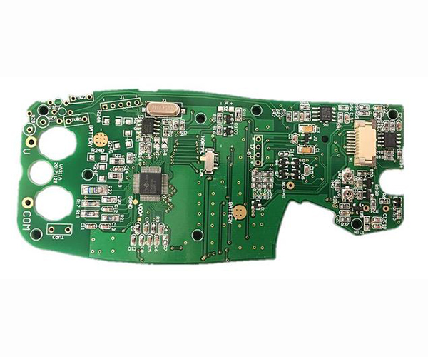
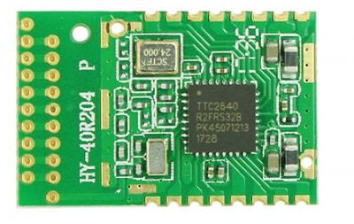
Designing a good PCBA board is our fundamental source. The electrical principle and mechanical structure design are used to determine the size and structural shape of the PCBA according to the structure of the whole machine. Draw the outline process drawing of the SMT printed board, mark the length, width, thickness of the PCB, the position and size of the structural parts, assembly holes, and leave the edge size, so that the circuit designer can carry out the wiring design within the effective range. The choice of assembly form depends on the type of components in the circuit, the size of the circuit board and the equipment conditions of the production line. The selection principle of the assembly form of the printed board: Follow the principle of optimizing the process, reducing the cost, and improving the quality of the product. First determine the overall goal of the electronic product function, performance index, cost and the overall size of the whole machine. Positioning of product performance, quality and cost.

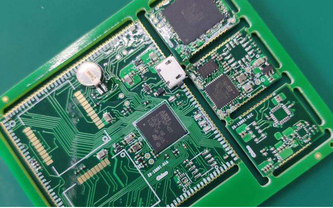
-Under normal circumstances, any product design needs to weigh and compromise between performance, manufacturability and cost. Therefore, the purpose and grade of the product must be positioned first when designing. The PCB board design is complicated, and various unexpected factors often affect the realization of the overall solution. How can we overcome these different problems? How do we draw a clean, efficient and reliable PCBA board? We are a professional PCB design company. PCBA board design seems very complicated. It is necessary to consider the direction of various signals and the transmission of energy. But in fact, the summary is very clear and can be started from two aspects: frankly speaking, it is: "how to put it" and "how to connect". 1. Follow the layout principle of "big and small first, difficult and easy first", that is, important unit circuits and core components should be given priority. This is like eating a buffet: the appetite of the buffet is limited to picking favorite foods, and the PCB board design space is limited to picking important pendulums. 2. The layout should refer to the schematic diagram and arrange the main components according to the main signal flow direction of the PCB board design. . The layout should try to meet the following requirements: the total connection should be as short as possible, and the key signal line should be the shortest; the layout of the decoupling capacitor should be as close as possible to the power supply pin of the IC, and the loop formed between the power supply and the ground should be as short as possible; Prevent accidents on the road. 3. The arrangement of components should be easy to debug and repair, that is, there should be no large components around small components, there must be enough space around the components to be debugged, and the situation of overcrowding will often become very embarrassing. The heating elements should be roughly evenly distributed. In order to facilitate the heat dissipation of the single board and the whole machine, the temperature sensitive elements other than the temperature detection elements should be kept away from the elements with high heat. 5. For the circuit part of the same structure, adopt the "symmetrical" standard layout as much as possible; optimize the layout according to the standard of uniform distribution, balanced center of gravity, and beautiful layout. 6. Plug-in components of the same type should be placed in one direction along the X or Y direction. The same type of polar discrete components must also be consistent in the X or Y direction to facilitate production and inspection. 7. High-voltage, high-current signals are separated from low-current and low-voltage weak signals; analog signals are separated from digital signals; high-frequency signals are separated from low-frequency signals; the interval of high-frequency components is sufficient. When handling components, consider that devices that use the same power source should be placed together as much as possible to facilitate future power source separation. The main consideration of the "how to place" layout. And "how to connect" is relatively more complicated, the priority of key signal lines: analog key signal priority routing, such as small signals, high-speed signals, clock signals and synchronization signals; the principle of density priority: start wiring from the most complex device designed on the PCBA board. Route the wiring from the densest area of the board.
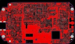
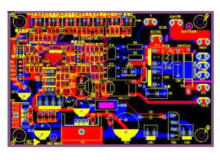
Wiring is an important step in PCB product design. The wiring design process is the most rigorous, the skills are the best, and the workload is the greatest. It can be said that the previous preparations have been completed. PCBA layout is divided into three types: single-sided wiring, double-sided wiring and multilayer wiring. PCBA layout can be completed using automatic and manual routing provided by the system. Although the system provides designers with convenient operation and automatic routing with high routing rate, there are still unreasonable places in the actual design. At this point, the designer needs to manually adjust the wiring on the PCBA to obtain the best results. The quality of PCBA design has a great influence on its anti-interference ability. Must comply with the basic principles of design, and should meet the requirements of anti-interference design, in order to achieve the best performance of the circuit.
The printed PCB wire should be as short as possible; the address wire or data wire of the unified component should be as long as possible; when the circuit is a high-frequency circuit or the wiring is dense, the corners of the printed wire should be round. Otherwise, it will affect the electrical characteristics of the circuit. When double-sided wiring, the wires on both sides should be perpendicular to each other, skewed or bent to avoid being parallel to each other to reduce parasitic coupling. PCB should use 45° fold lines instead of 90° fold lines to reduce the coupling of external transmission and high frequency signals. As the input and output of the circuit, printed wires should be avoided as much as possible to avoid backflow, and it is best to add grounding wires between these wires. When the board surface wiring density is high, the mesh copper foil should be filled with a grid size of 02mm (8mil).
SMD pads cannot be placed through holes to avoid loss of solder paste caused by component solder joints. It is not allowed to pass important signal lines between sockets. Avoid horizontally mounted resistors, inductances (insertions), electrolytic capacitors and other components under the hole to avoid short circuit between the hole and the component shell after peak welding. When wiring manually, put the power cord on the ground wire first, and the power cord should be on the same level. The signal line cannot have loopback wiring. If a loop is necessary, try to make the loop as small as possible. When wiring passes between two pads without connecting to them, they should maintain a large and equal spacing. The distance between wiring and wires should also be uniform, equal and maximum. The connection between the wire and the pad should be too smooth to avoid small sharp corners. When the center distance between the pads is smaller than the outer diameter of one of the pads, the width of the connecting line between the pads can be the same as the diameter of the pad; when the center distance between the pads is greater than the outer diameter of the pad, The width of the welding wire should be reduced; when there are more than 3 pads on the wire, the distance between them should be greater than the width of the two diameters. The common ground of the printed wire should be placed on the edge of the PCB as much as possible.
The copper foil should be kept on the PCB as much as possible, so that the shielding effect is better than the long grounding wire. It will also improve the transmission line characteristics and shielding effect, and also realize the function of reducing distributed capacitance. The common ground of the printed conductors preferably forms a ring or net, because when there are many integrated circuits on the same PCB, a ground potential difference is generated due to the limitation of the pattern, which leads to a reduction in noise tolerance. When a loop is formed, the ground potential difference decreases. In order to suppress noise, the ground and power modes should be as parallel as possible to the flow of data. Multi-layer PCBA can use several layers as shielding layers. The PCB power layer and PCB ground layer can be regarded as shielding layers.