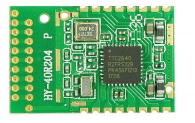
1. Case background
The sample submitted for inspection is a PCBA board. After the PCB board has been SMT, it is found that a small number of pads have poor tinning. The failure rate of the sample is about three thousandths. The surface treatment process of the PCB board pad is chemical tin-immersion, the PCB board is a double-sided patch, and the pads with poor soldering are all located on the second patch surface.
2. Brief description of analysis methods
2.1 Observation of sample appearance
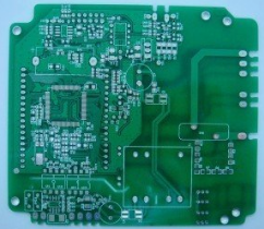
As shown in Figure 1, through the microscopic observation of the failed pad, there is no tin on the pad, and no abnormal conditions such as obvious discoloration are found on the surface of the pad.
Failure analysis of poor tin on PCB pads
2.2 SEM+EDS analysis of the pad surface
Surface SEM observation and EDS component analysis were performed on NG pads, once-fired pads, and un-fired pads. The surface of the un-fired pads was formed well, and the surface of the once-fired pads and failed pads were tin-immersed. The layer recrystallized, and no abnormal elements were found on the surface;

2.3 Analysis of the FIB sample preparation profile of the pad
Use FIB technology to make cross-sections of failed pads, once-fired pads and non-fired pads, and scan the surface of the profile. It is found that Cu elements have appeared on the surface of the NG pad, indicating that Cu has diffused to the surface of the tin layer; Cu element appears on the surface of the furnace pad at a depth of about 0.3μm, which means that the thickness of the pure tin layer is about 0.3μm after the furnace pad. The thickness of the pure tin layer of the furnace pad is about 0.8 μm. In view of the low accuracy of the EDS test and the relatively large error, the next step is to use AES to further analyze the surface composition of the pad.
2.4 AES composition analysis of the pad surface
Analyze the polar surface composition of the NG pad and the once-fired pad. The NG pad is in the depth range of 0~200nm, mainly Sn and O elements, and in the depth range of 200~350nm, it is a copper-tin alloy, which is almost non-existent. Pure tin layer; the solder pad is mainly tin layer in the depth range of 0~140nm once after the furnace, after which the element Cu (metal compound) appears
3. Analysis and discussion
Based on the above analysis results, the reasons why the solder pad cannot be tinned are summarized as follows:
a). The pure tin layer on the surface of the NG pad has been completely consumed (the surface layer is oxidized, and the inside is transformed into intermetallic compounds), which cannot meet the requirements of good solderability;
b). When the pad passes through the furnace once, the high temperature will promote the mutual diffusion of tin and copper to form an alloy layer, resulting in the thinning of the pure tin layer;
c). The NG pad has been through the furnace once before SMT placement. During the furnace process, the surface tin will be oxidized. At the same time, the high temperature will aggravate the mutual diffusion of tin and copper to form a copper-tin alloy and thicken the copper-tin alloy layer., The tin layer becomes thinner. When the thickness of the tin layer is less than 0.2μm, the pad will not be able to guarantee good solderability, and poor tin application failure will occur.
4. Suggestions
(1) Use nitrogen as the SMT protective atmosphere;
(2) Increase the thickness of the tin-immersion layer of the PCB board to ensure that the thickness of the tin layer can still meet the solderability requirements after the furnace is passed once.
5. Reference Standard
(1) GJB 548B-2005 Microelectronic device test methods and procedures Method 5003 Microcircuit failure analysis procedures
(2) IPC-J-STD-003B-2007 PCB solderability test method