Wafer level chip size Packaging (WLCSP) technology application status and market prospect analysis in 2021.
Advanced IC Packaging refers to the most cutting-edge packaging form and technology at that time. At present, packaging with flip chip (FC) structure, wafer level packaging (WLP), 2.5D packaging, 3D packaging are considered as advanced packaging category.

Advanced packaging development circuit diagram
The overall semiconductor packaging market is expected to grow in revenue at a compound annual growth rate (CAGR) of 5.2% from 2018 to 2024, while the advanced packaging market is expected to grow at a CAGR of 8% and the market size will grow to $40 billion by 2023. The traditional packaging market, on the other hand, is growing at a cagR of less than 3.3%. Among the various advanced packaging platforms, 3D silicon through hole (TSV) and fan-out (FAN-out) packages will grow by 29% and 15%, respectively. Flip-chip packages, which account for the majority of the advanced package market, will grow at a compound annual growth rate of about 8 per cent. Fan-in WLP, meanwhile, will also grow at a CAGR of 8 per cent, driven mainly by the mobile market.
Global Advanced Packaging Technology Market Size forecast, 2018-2024 (us $1 billion)

In addition, there is a growing trend to combine front-end wafer manufacturing with advanced back-end packaging. Major global wafer manufacturers (such as Intel, TSMC and Samsung) have closely combined advanced wafer manufacturing technology with advanced packaging forms to strengthen the technology integration advantages of IC product manufacturing. Influenced by both technology and scale, the concentration of the global sealing and testing industry has steadily increased. Before 2017, eight sealing and testing enterprises (including the back-end packaging business of founds) occupied about 87% of the advanced packaging market share.
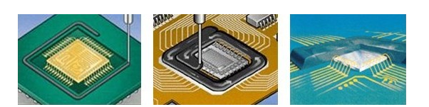
Wafer level chip size Packaging (WLCSP), as a kind of advanced packaging technology, meets the needs and trends of consumer electronics development (light, small, short, thin and low price). Compared with traditional packaging, WLCSP packaging has the following main advantages: (1) WLCSP optimized the packaging industry chain. In the traditional packaging method, the wafer is first sliced into a pellet chip. After being tested as a qualified chip, the wafer is placed on the lead frame or packaging substrate (substrate), and then the packaging test is carried out. The industrial chain involves the wafer factory, substrate factory, sealing factory and testing factory. The wafer size packaging is to encapsulate and test the wafers, and then cut the wafers after the encapsulation and test. Compared with traditional packaging, WLCSP packaging can integrate the substrate factory, packaging factory and test factory in the traditional packaging industry chain into one, so that the chip production cycle is greatly shortened, the production efficiency is improved, and the production cost is reduced. Secondly, WLCSP package can reduce the testing of qualified chips before packaging, and can effectively reduce the packaging cost; Finally, THE WLCSP package is an extension of wafer manufacturing technology, which greatly reduces the technical difference between the semiconductor back segment (packaging) and the front segment (wafer manufacturing), making it easy to realize the technical docking between the semiconductor back segment and the front segment. WLCSP packaging can integrate IC design, wafer manufacturing, packaging testing, substrate factory into one, optimize the industrial chain, solve the problem of technical and standard docking in IC design, wafer manufacturing, packaging testing, substrate factory and other links, and further promote the development of professional foundry mode.
Number of wafers using advanced packaging (equivalent to 12 inches) and distribution by business model in 2018

2. The packaging cost decreases with the increase of the number of chips on the wafer. Wafer level chip size packaging is to package the entire wafer and then cut the chip, while the traditional packaging is to cut the wafer into the chip first, and then implement the chip packaging. Generally speaking, the packaging cost of WLCSP is measured according to the number of wafers, and the number of chips after cutting is not necessarily related to the traditional packaging packaging cost is measured according to the number of encapsulated chips. Therefore, the packaging cost of WLCSP decreases as the wafer size increases and the number of chips increases. In the consumer electronics market development trend of light, small, short, thin, wafer level chip size packaging cost advantage is more obvious, will gradually usurp the traditional packaging market share.
3. WLCSP will become the mainstream packaging method in the future. The industry believes that 3d packaging technology based on silicon through hole (TSV) is the main solution beyond Moore's Law, and is the future development trend of semiconductor packaging technology. WLCSP packaging is the basis of silicon through hole technology, and the two processes are very similar. By mastering WLCSP packaging technology (especially Shellcase series WLCSP), we can quickly enter the field of silicon through hole technology and play a major role in the future 3D packaging technology.
The difference between wafer level chip size package and traditional package

Yole Development forecasts that the WLCSP package market will grow from approximately $1.4 billion in 2010 to $3.2 billion in 2018 at a compound annual growth rate of 12%, accounting for approximately 11% of advanced packages and approximately 6% of the global closed beta industry. Driven by demand for small size chips such as consumer electronics and automotive electronics, we expect the WLCSP package market to reach approximately $3.5 billion in 2019, with further growth expected.
WLCSP mainly adopts wafer bump packaging and Shellcase series WLCSP packaging technology. Wafer bump package is a form of WLCSP package with relatively low technical difficulty. Its main feature is that the circuit and welding pad can be directly led out on the front of the chip. Shellcase series WLCSP can not only lead the circuit and welding pad directly on the front of the chip, but also lead the circuit of the chip to the back of the chip and then make the welding pad. Shellcase series WLCSP package includes the key technical points of the wafer bump package, which is more difficult than the wafer bump package, and the process is more complex than the wafer bump package. Due to the significant differences in technical difficulties and application fields, the unit price of wafer bump packaging technology is lower than Shellcase series packaging technology. Shellcase series WLCSP has excellent advantages in image sensor packaging, while wafer bump packaging cannot be applied to image sensor and other fields because of the welding pad on the front of the chip.
IPCB Circuit is a professional high precision PCB circuit board R & D manufacturer, can batch produce 4-46 layer PCB board, circuit board, circuit board, high frequency board, high speed board,HDI board, PCB circuit board, high frequency high speed board,IC seal loading board, semiconductor test board, multi-layer circuit board,HDI circuit board, mixed voltage circuit Board, high frequency circuit board, soft and hard board, etc.
In 2018, the size of the packaging substrate market was nearly $7 billion