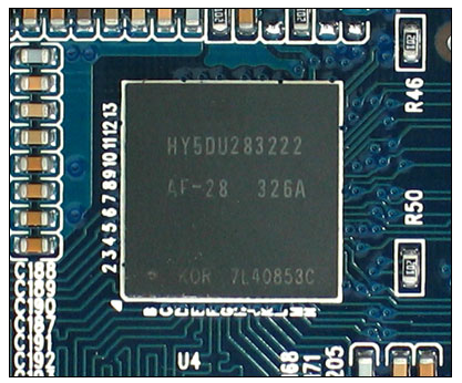
When the line width and line spacing of PCB are less than 50 uM (2mil), the traditional CCL Subtractive Process (SP) is almost useless. Now, the line/width of CSP or FC cladding and other carrier plates is approaching 15 μ m/15 μ m. In terms of mass production of large row of plates, only insulated plates without copper foil coating can be selected as the starting point of mSAP (Semi-Additive Process) semi-additive method.
Production process of mSAP (Semi-Additive Process)
Inner layer - ABF laminaTIon - Laser drill - Electroless CU Seed layer - Photo resist patterning - ElectrolyTIc Cu plaTIng - Photo resist removal - Seed layer etching
")
1. Structure of ABF thin material
On the large double-sided (or four-layer) inner thin core plate (core thickness 2.5mil) with completed circuit and black oxidation treatment, the B-Stage ABF film plate with white copper-free but polyester protective film (Mylar, Polyester) is vacuum pressed on both sides, and then it needs to be hardened at 180 ℃ for 30 minutes. This ABF (Ajinomoto Bond Film) is a high-priced plate of the "Taste Essence Fine Technology" company (AFT) under the Japanese company "Dayun Taste Essence". There are three kinds of current products:
A. General SH9K (Tg165 ℃, TMA)
B. Halogen-free GX-3 (Tg153 ℃)
C. Halogen-free low Z-expansion large GX-13 (Tg156 ℃) а The Z swell of 2 is only 155 ppm/℃.
Note that the AFT company not only launched the common ABF products in the carrier category, but also introduced the 2L type base material of ABF-XA5 and the 3L type base material of ABF-LE-T in the softboard industry.
2. Vacuum film pressing
First, the inner core board shall be completed according to the traditional multi-layer board manufacturing process, and then the resin hole and the whole board surface shall be completely flattened to facilitate the double-sided bonding of ABF thin materials. According to the materials on the website of Ajinomoto Fine Techno (AFT), the ABF three-layer material cut by the active film cutting machine is like a dry film type, and then the vacuum-type active film sticking machine is used. First, the ABF two-layer material with the barrier removed is pasted on both sides of the inner core plate. The temperature of the continuous vacuum film is about 110 ℃ for about 30 seconds, and then the hot pressing bed is used to flatten and solidify the film for 60 seconds under the high pressure of 110 ℃ and 5kgf/cm2. After that, the Mylar (PET) transparent maintenance film can be removed and the post-hardening work of the attached ABF film material can be continued. Take GX13 as an example, it needs another 30 minutes of curing (Cure) at 180 ℃ to calculate the completion of the additional layer.
3. Laser hole-forming and full-board glue removal
The film thickness of ABF after aging is about 30-70 um, 30~40 for thin plate um Compared with 2-4mil fired holes completed by general double-sided CO2 laser, the hole shape can appear excellent inverted cone shape. After the desmearing of the whole plate without copper surface, the whole plate surface and hole wall can form a very rough appearance, and the chemical copper will help the adhesion of the dry film of the fine line.
There is no big difference between the action of removing the glue residue of the crystal carrier plate and that of the general PCB. It is still three stations, namely, pre-swelling, manganese (Mn+7) sol and neutralization and recovery. The difference is that the general PCB only deals with the hole wall area of through-hole or blind hole, but in addition to the hole wall of the blind hole, the whole board ABF surface needs to be expanded and etched, in order to make 1u The m thick copper layer (more than twice as thick as the general PCB) is rougher in appearance, which makes the dry film photoresist and copper electroplating obtain better adhesion in large-area fine wire operation.
4. The difference of mSAP semi-addition method for rubber slag removal
Generally, the glue removal slag of the multi-layer plate is only for PTH or μ- Via and other hole walls, the total area of treatment is not large. However, the SAP method not only deals with the micro-blind-hole wall, but also responds to the two large plates with no copper on the surface. The huge difference between the two cannot be handled on the same site. The first thing that needs to be changed is the timely electrolytic oxidation of Mn+6 to keep the minimum effect of the bath liquid; The second is how to remove the recovered Mn+4 precipitates in the high-temperature bath solution; The third is how to clean up the accumulated Na2CO3 generated by the reaction of strong alkali tank liquid to generate CO2. At present, there is no outstanding method to deal with the solid problems such as Mn+4 and Na2CO3, and only part of the tank liquid can be poured according to the total area treated. Of course, we should also refer to the specific gravity of the tank liquid to control the total amount of Na2CO3 to determine whether it is necessary to replace a new tank. It can be seen from this that the cost of SAP is by no means comparable to that of general PCB degumming slag.
The difference between ABF film material and hard board is that after neutralization and recovery, a process of biting off fillers such as SiO2 or glass beads should be added to increase the external surface area to ensure the grip of subsequent copper layer. The defect is that the dead angle of the plate increases significantly, resulting in the subsequent etching of the bitten copper layer to form an independent line, while the noble metal palladium layer for activation will still remain in the plate, burying the hidden worry of poor insulation between fine lines. Especially when the outer panel is maintained with a thin layer of green paint, it is inevitable that insulation failure will occur during long-term operation in high temperature and humidity environments, and even lead to the problem of signal integrity.
5. Low-stress chemical copper before photoresist imaging
ABF appearance completion 2 μ After m chemical copper, dry film photoresist can be pressed and pasted, and then exposed and developed to obtain many lines and many blind holes (18 × The two sides of the 24 "board are usually more than 800000 blind holes) in the copper plating base for copper plating and copper filling of the blind holes. The electroplating copper here is equal to the secondary copper of the general PCB, while the chemical copper layer is like the chemical copper and primary copper added on the CCL copper foil of the general PCB.
It can be seen that chemical copper of SAP method plays a more important role than chemical copper of general PCB, and its thickness is also required to be added to 1! one point five μ M is at least twice as much as usual. In order to obtain better adhesion, the copper layer here also pays special attention to the promotion of crystal growth and stress reduction; Not only the production rate will be slower (less than half of the conventional copper), but also the cost of various chemicals of CP grade will increase more than three times. The general HDI multilayer board can't afford it now, as long as the FC carrier board can reluctantly choose this kind of high grade and low stress chemical copper with high unit price.
6. Electroplated copper after dry film imaging
The copper plating used by SAP is the same as that used by ordinary HDI to fill blind holes. It is a high-speed copper plating with low aspect ratio and non-deep hole. In other words, it is short hole copper plating with little attention to elongation and tensile strength. In the ELIC-dominated market of repeatedly adding layers and filling blind holes, the main demand of these repeated high-speed copper plating is "fast". However, under the restriction of the natural generation of the limited current density (Jlim) of acid copper plating, the substrate can not pull up the voltage to increase the current, as long as it is close to the gap between the anode and cathode in the copper bath as possible (the vertical hanging plating has been shortened from 20 cm to 5~10 cm, and the horizontal walking plating is more urgent to 2 cm), the resistance of the copper float can be reduced below to reach above the available current density. At the same time, the resistance and current can be decreased by increasing the temperature of the bath liquid (from 20 ℃ to 40 ℃). However, in this way, soluble copper balls cannot be continuously used to maintain the stability of the interval between the anode and cathode. Therefore, titanium class insoluble anodes are widely used in the field of hole-filled copper plating. However, insoluble anodes suffer from various disasters of oxygen, especially the cracking and overuse of organic additives, especially the carrier with the largest amount. Therefore, the total organic compound (TOC) of the fatal injury of the bath solution is rising steadily. In order to maintain the minimum quality of copper plating, we have to pour part of the bath solution on time (pour 1/10 of the bath solution every week), only to make up for DI water to restrain the rising TOC. As for the rapid consumption of titanium anode and the compensation of copper oxide have become the other two negative factors of cost. The difference between the traditional deep hole slow copper plating and the new blind hole fast copper filling depends on which attitude.
7. Finish the line after biting off part of the copper
After the completion of the copper plating process of filling blind holes and thickening lines, the photoresist can be removed and the overall etching can be carried out directly. At the moment, the chemical copper in the non-line insulation area on the board is very easy to be removed, so the copper plating of the line will certainly be worn away without any indiscriminate and comprehensive corrosion, but it will not hurt the elegance. The thin lines are not only oily on the shoulders, but also the residual feet at the bottom disappear. The quality is better! This method is called Differential Etching.
8. Abnormal color of adjacent OSP pad
All kinds of plates processed by OSP often have different shades of brown on the two pads of some capacitors. Through solderability tests and mass production by inferior customers, there is no problem of poor solder joints. However, persistent customers are still chasing after each other and constantly asking for real causes and improvements. PCB manufacturers will also try all kinds of methods and even track down the liquid medicine suppliers. Without any solution, it is inevitable to question whether there is any problem in the planning and layout. They want to kick the ball back to the client to get out of trouble. However, in the absence of evidence, we have to admit our mistakes and settle claims in all kinds of ways to solve the dispute.
9. Quantification of copper bite
In order to further understand how much the three pads of electroplating copper layers were bitten off in the OSP process and how different the thickness was, the software of the microscope was deliberately used to measure the thickness of the three pads of copper for comparison.
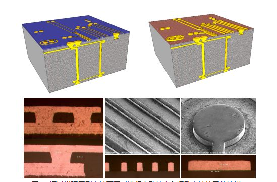
In addition to the thickness measurement of such micro-section software, WyCo's fine roughness measuring instrument can also be used to measure the two types of copper pads marked on the surface of the electrode material, so as to prove the correctness of the inference again. According to the data obtained, the uniform copper height of the independent dark pad is 29.1 μ m. The uniform copper height of the interconnection blind hole light-colored pad is 25.3 μ m。 Note that the blue color in the next two pictures shows the appearance of the lowest plate. The green color is the height of the copper pad, and the red color on the outer edge is the higher green paint.
10. Formation of OSP film
The clean copper surface is first dissolved into Cu+1 in the OSP tank solution equipped with formic acid or acetic acid, and this monovalent copper ion will immediately complexe (stagger) with the organic substance Imidazole in the liquid medicine to form a brown organic film and gradually thicken. The above-mentioned light copper pad with blind holes is fast and fierce in biting copper, which causes part of its univalent copper to be rapidly oxidized into blue divalent copper and enter the bath liquid without forming a film. As a result, the thickness of its skin film is unavoidably inferior to that of the independent pad, so there is a fierce contrast between dark and light colors.
Here we share the method of mass production of IC substrate in mSAP process.