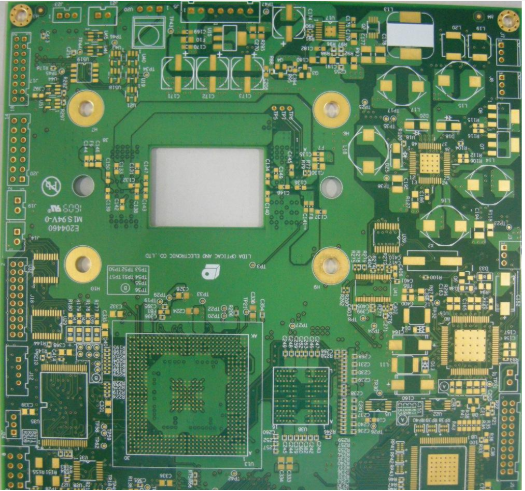
The design of PCB single-sided circuit boards requires exposure to many professional data and some physical knowledge, which can be said to be a comprehensive skill project. If you want to make a high-quality circuit board, you need not only a solid foundation, but also sensitivity to impedance. The impedance involved in the PCB board mainly includes the following aspects:

When the direct current of the printed PCB circuit board passes through the wire, it will encounter a resistance. This resistance is called resistance, which corresponds to R, and the unit of value is "ohm" (Ω).
The relationship between resistance and current and voltage is: R=V/I
In addition, the resistance is also related to the resistivity (β) of the conductor material, the length of the wire (L), and the cross-sectional area (S) of the conductor. R = β L/S
Advertising Taobao, PCBA washing machine, preferred fashion goods, super value purchase, PCBA washing machine, quality assurance, enjoy life, all on Taobao! ^^ On Taobao, I like it! Discount Amoy...
1, resistance
When an AC current flows through a conductor, the resistance encountered is called Impedance, which corresponds to Z, and the unit is still Ω.
The resistance at this time is different from the resistance encountered by the DC current. In addition to the resistance of the resistance, there are also the resistance of inductive reactance (XL) and capacitive reactance (XC).
is the resistance of the differential direct current, and the resistance encountered by the alternating current is called impedance (Z).
Z=√ R2 +(XL -XC)2
2, impedance (Z)
In recent years, with the improvement and application of IC integration, the signal transmission frequency and speed are getting higher and higher. Therefore, in the printed board wire, after the signal transmission (emission) reaches a certain value, it will be affected by the printed board wire. Its own influence, resulting in severe distortion or complete loss of the transmitted signal. This shows that the "thing" "circulated" by the PCB wire is not current, but the transmission of square wave signals or pulses in energy.
The resistance encountered during transmission of the above-mentioned “signal” is also called “characteristic impedance”, and its symbol is Z0.
Therefore, it is not enough to solve the problems of "on", "off" and "short circuit" on the PCB wires, but also to manipulate the characteristic impedance of the wires. In other words, transmission lines for high-speed transmission and high-frequency signal transmission are much stricter in quality than transmission wires. It is no longer the "open circuit/short circuit" test passed, or the gap or burr does not exceed 20% of the line width, it can be accepted. It must be required to determine the characteristic impedance value, and this impedance must also be controlled within the public service, otherwise, it will only be invalidated and not reworked.
The characteristic impedance Z0 of the multi-layer board signal transmission line is now required to control the scale usually: 50Ω±10%, 75Ω±10%, or 28Ω±10%.
To control the scale of change, four factors must be considered:
(1) signal line width W;
(2) Signal wire thickness T;
(3) the thickness of the dielectric layer H;
(4) Dielectric constant εr.
The greatest influence is the thickness of the dielectric, followed by the dielectric constant, the width of the wire, and the smallest is the thickness of the wire. After the substrate is selected, the change in εr is small, the change in H is also small, and T is easier to manipulate, but it is difficult to control the line width W at ±10%, and the line width problems include pinholes, notches, dents, etc. on the wire problem. In a sense, the most effective and important way to manipulate Z0 is to manipulate the line width.
Grasping the data of these physical properties will be of great assistance to PCB design. Experienced and skilled personnel will consider all PCB factors and avoid quality problems in the end. This is not just relying on experience, but more on a sufficient understanding of physical properties.