Take you to understand the process from bare PCB to PCBA
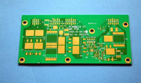
The Chinese name of PCB (Printed Circuit Board) is printed circuit board, also known as printed circuit board. It is an important electronic component, a support for electronic components, and a carrier for electrical connection of electronic components. Because it is made by electronic printing, it is called a "printed" circuit board.
PCBA (Assembly of PCB) is the whole process of PCB empty board after SMT patch, and then DIP plug-in, referred to as PCBA. PCBA is a common way of writing in China, while the standard way of writing in Europe and America is PCB'A, with an oblique dot added.
The above two terms have already been understood, so do you probably know the process from PCB bare board to PCBA?
Yes, the process is the PCBA after the bare PCB board passes through the SMT patch and then to the DIP plug-in. However, this PCBA must be a PCBA that has no problem after a test process.
Let us walk through the process from bare PCB to PCBA, and feel the "threat" of machines to humans!
SMT placement process

SMT (Surface Mounted Technology) is a surface mount technology (Surface Mounted Technology), which is one of the most popular technologies and processes in the electronics assembly industry.
Simply put, it is a kind of surface mount components without leads or short leads (SMC/SMD for short, chip components in Chinese) mounted on the surface of a Printed Circuit Board (PCB) or the surface of other substrates Above, the circuit assembly technology that is assembled by soldering and assembling by reflow soldering or dip soldering.
So what preparations need to be made before SMT placement?
1. There must be a MARK point on the PCB, also called a reference point, which is convenient for the placement of the placement machine and is equivalent to a reference object;
2. To make a stencil to help the deposition of solder paste, transfer the exact amount of solder paste to the exact position on the empty PCB;
3. SMD programming, according to the provided BOM list, the components are accurately positioned and placed in the corresponding position of the PCB through programming.
After all the above preparations are completed, SMT patch can be carried out.
First of all, the placement machine determines whether the board's feeding direction is correct according to the MARK point on the incoming board, and then brushes the solder paste on the stencil, and deposits the solder paste on the PCB pads through the stencil.
Next, the placement machine places the components on the corresponding positions of the PCB board according to the placement programming, and then undergoes reflow soldering to effectively contact the components, solder paste and the circuit board.
Finally, automatic optical inspection is carried out to check the components on the PCB board, including: virtual soldering, solder connection, device orientation, etc., but the functional inspection cannot be done because the board has plug-in components that have not been soldered.
It should be noted that some devices have positive and negative poles or pin order, so it is necessary to check the incoming materials to prevent patch errors, especially for BGA packaged devices. If the direction is wrong, subsequent disassembly and repair soldering are compared Time-consuming and laborious.