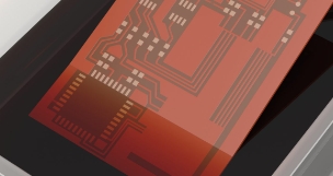
The etching solution is a special chemical agent commonly used for etching circuit boards, semiconductor chips, metal components, and other fields, which can achieve the purpose of removing or changing the surface properties of materials.

PCB etching solution
Etching is an important process in the manufacturing of printed circuit boards, and a large amount of high copper etching waste is generated during the production process of circuit board factories.
At the beginning of the process, a complete copper foil is attached to the substrate, the electrical circuit is engraved on it, and tin is attached to it to ensure that the electrical circuit is not etched off, ensuring the integrity of the copper that makes up the electrical circuit. Chemical etching has become an indispensable step in the process of printed circuit boards. Nowadays, etching solutions used in industrial production should possess the following six technical properties:
1) The etching solution should ensure the performance requirements of the corrosion-resistant protective layer or the electroplating-resistant protective layer from being etched.
2) The etching process has a wide range of conditions (temperature, external environment, etc.), a relatively good working environment (without too much volatile toxic gas), and can effectively implement automatic control.
3) The etching effect is relatively stable and has a long service life.
4) The etching coefficient is high, the etching speed is high, and the side etching is small.
5) Has a significant ability to dissolve copper.
Process flow of circuit board etching
The process of printing circuit boards from light boards to displaying circuit patterns is a relatively complex physical and chemical reaction. This article analyzes the final step - etching. At present, the typical process for processing printed circuit boards adopts the "graphic electroplating method". First, a lea-tin corrosion-resistant layer is pre-coated on the copper foil part that needs to be retained on the outer layer of the board, which is the graphic part of the circuit. Then, the remaining copper foil is chemically corroded off, which is called etching.
After graphic electroplating, the board enters the etching process, which is divided into three small steps: film removal, etching, and tin removal.
1) Firstly, perform film removal. The film removal solution in the machine will remove the exposed dry film on the board. After the dry film on the board disappears, copper will be exposed, but this copper is not what we need. The copper we need is underneath the tin, and then the board enters the etching process. The chemical solution only reacts with the copper and does not affect the tin. Therefore, the exposed copper will be corroded off, including the inner layer of the multi-layer board and the outer layer of the single and double boards, Acidic or alkaline corrosion solutions can be selected based on process requirements and characteristics.
2) In general, acidic etching solution is more suitable for the inner layer, while alkaline etching solution is more suitable for the outer layer. After etching, only the tin is left on the circuit board (the tin needs to be removed), and the board will enter the tin removal process as the roller moves. Here, a chemical solution will be used to dissolve the tin layer on the circuit board, restoring the original color of copper to the circuit board.
3) After the etching process is completed, it goes to the next process - AOI testing. The PCB is placed in dedicated testing equipment, and the surface of the PCB is scanned using ultra-clear optical cameras and graphics processing systems to obtain high-definition images for analysis and comparison. Possible defects and problems are detected, and they are corrected and optimized. After being determined as a good product, it will proceed to the next process - solder mask.
Etching solution has a wide range of applications in industry and can be used in many fields such as semiconductors, electronics, and metal processes. When using an etching solution, an appropriate etching solution should be selected and temperature and time should be strictly controlled. Attention should be paid to waste liquid treatment and personal safety to fully utilize the function of the etching solution.