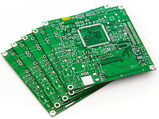
The opening of fr4 pcb BGA welding can be caused by several factors, including insufficient solder paste, poor solderability, poor coplanarity, mounting misalignment, thermal mismatch and exhaust through the solder mask. The effects of various factors are described as follows.
1. Insufficient solder paste
Inadequate solder paste printing caused by opening blockage will cause solder opening, which is very common in CBGA or CCGA, because solder paste collapse will not occur during reflow of these two devices.

2. Poor weldability
The pad contamination and oxidation usually cause wetting problems. If the fr4 pcb pad is contaminated, because the solder cannot be wetted with the fr4 pcb pad, under the capillary action, the solder flows to the interface between the solder ball and the component, and the fr4 pcb pad side will form open welding. Poor weldability of the pad will also cause weld opening after the PBGA solder ball melts and collapses.
3. Poor coplanarity
Poor coplanarity usually induces or directly causes weld opening, so the maximum value of fr4 pcb non-coplanarity cannot exceed 5mil in local area or 1% in the whole area (the acceptable category in IPC-600 standard is D, and the grades are 2 and 3). In the repair process, the preheating process should be adopted to minimize the non-coplanar deformation of fr4 pcb.
4. Chip offset
The deviation of the component during mounting will usually cause the opening of welding.
5. Thermal mismatch
The shear force caused by internal stress will cause the weld opening. Under specific process conditions, when a large temperature gradient passes through the fr4 pcb, this phenomenon of weld opening will occur. For example, SMT reflow is often followed by wave soldering. The BGA corner solder joint formed in the reflow will crack from the interface between the solder joint and the packaging component in the wave soldering stage. In some cases, the solder joint at the corner of BGA is still connected to the component and the fr4 pcb pad. In fact, the pad and the strip from the fr4 pcb are only connected to the negative line of the fr4 pcb. In both cases, the solder joint of BGA is close to the through-hole position.
The root cause of this phenomenon is that there is a large temperature gradient from fr4 pcb to packaging. In wave soldering, molten solder reaches the top surface of fr4 pcb through the through-hole, resulting in rapid temperature rise on the top surface of fr4 pcb. Because solder is a good thermal conductor, the temperature of solder joint rises rapidly. On the contrary, the package itself is not a good thermal conductor, and the heating process is very slow.
The mechanical strength of solder in molten state is reduced. Once thermal mismatch occurs, stress will be generated between hot fr4 pcb and cold PBGA, and cracks will be generated between package and pad. In some cases, the adhesion strength between the pad and the fr4 pcb is lower than the connection strength between the solder encapsulation pad, which will cause the peeling of the fr4 pcb and the pad. Since the corner solder joint is far from the center point, the thermal mismatch is more significant and the stress is greater. The problem can be solved by printing the solder mask on the through-hole. This method produces much less open welding than through holes without covering. If the production volume is not large, a layer of high-temperature adhesive tape can also be manually pasted on the through-hole before wave soldering to isolate the heat transfer path and solve the problem of welding opening.
6. Exhaust gas passing through the solder mask
For BGA pads with solder mask restrictions around them, poor exhaust will also cause weld opening. At this time, the volatiles will be forced to discharge from the interface between the solder mask and the packaging pad, so the solder will be blown away from the packaging pad to form weld opening. This problem can be solved by pre-drying the BGA patch.
To sum up, the following measures can be taken to solve the problem of BGA welding opening:
1) Print enough solder paste
2) Improve the weldability of fr4 pcb pad
3) Maintain the coplanarity of fr4 pcb substrate
4) Precise mounting elements
5) Avoid excessive temperature gradient
6) Cover through hole before wave soldering
7) Pre-drying element