Heavy copper PCBs are widely used in various products because they provide multiple functions to improve circuit performance. These PCBs are widely used in high-power equipment such as transformers, heat sinks, inverters, military equipment, solar panels, automotive products, welding equipment, and distribution systems.

Heavy copper PCB
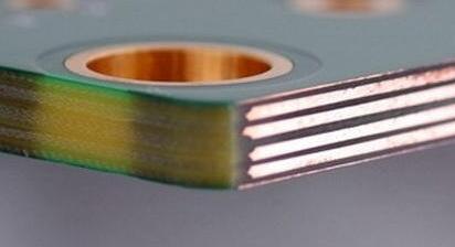
The heavy copper PCB structure
Standard printed circuit boards (PCBs), whether double-sided or multi-layer, are manufactured using a combination of copper etching and electroplating processes. The circuit layer starts with a thin copper sheet (usually ranging from 0.5 ounces per square foot to 2 ounces per square foot), which is etched to remove unwanted copper and plated to increase the thickness of copper, making it suitable for flat surfaces, wiring, solder pads, and plated through holes. Use an epoxy substrate (such as FR4 or polyimide) to press all circuits layer by layer into a complete package.
Circuit boards using heavy copper circuits are produced in the same way, while PCBs use specialized etching and electroplating techniques such as high-speed/step electroplating and differential etching. In history, heavy copper features were entirely formed by etching thick copper-clad laminate materials, resulting in uneven trace sidewalls and unacceptable undercutting. The advancement of electroplating technology allows for the formation of heavy copper features through a combination of electroplating and etching, resulting in straight sidewalls and negligible undercutting.
The construction of heavy copper PCB endows the circuit board with the following advantages
1. Increase tolerance to thermal strain.
2. Increase the current carrying capacity.
3. Increase the mechanical strength of the connector position and PTH hole.
4. Use special materials to fully utilize their potential (i.e. high temperature) PCB, without circuit failure.
5. Reduce product size by integrating multiple copper weights on the same layer of the circuit
6. The heavy copper plated via holes carry higher current from the PCB through the circuit board and helps transfer heat to the external heat sink.
7. Connectors are essential for jumper connections. However, connectors are often difficult to maintain on traditional PCBs. Due to the low strength of accidental PCBs, the connector area is usually affected by mechanical stress, but heavy copper PCBs provide higher strength, ensuring higher reliability.
Electroplated copper circuits enable circuit board manufacturers to increase the copper thickness on the side walls of plated and through holes. Now, it is possible to mix a PCB with standard functional copper on a single board (also known as PowerLink). The advantages include reducing the number of layers, low impedance power distribution, smaller footprint, and potential cost savings. Usually, high current/high power circuits and their control circuits are manufactured separately on separate circuit boards. Heavy copper plating makes it possible to integrate high-current circuits and control circuits to achieve high-density and simple PCB board structures. The heavy copper function can be seamlessly connected to standard circuits.
The industries that benefit from heavy copper printed circuit boards are military, defense, automotive, solar panel and welding equipment manufacturers, as well as other industries that require circuit boards capable of handling the complex heat generated today. Another heavy copper industry is industrial control. Heavy copper plated through holes is most suitable for transferring heat to external heat sinks. Efficient power distribution is crucial for ensuring the high reliability of PCBs, and heavy copper can achieve this.
Heavy copper is not an innovation as it has been used in PCBs for a long time and can withstand the strict requirements of military and national defense applications, such as weapon control. Mainstream electronic product manufacturers are increasingly demanding the transfer of heat from components, while heavy metals are becoming increasingly common in more and more nonmilitary applications.
Heavy copper plates are manufactured using electroplating and etching techniques, to increase copper thickness on the side walls of through holes and plating holes. If the circuit board undergoes multiple cycles during production, the plating holes will become weaker, and the addition of heavy copper will strengthen these holes. A circuit board made of heavy copper can achieve high currents, power, and control circuits on one circuit board.
Heavy copper PCBs are manufactured with 4 ounces or more of copper on each layer. 4-ounce copper PCB is most commonly used in commercial products. The concentration of copper can reach up to 200 ounces per square foot. Heavy copper PCBs are widely used in electronics and circuits that require high-power transmission. In addition, the thermal strength provided by these PCBs is impeccable. In many applications, especially in electronic products, the thermal range is crucial because high temperatures cause serious damage to sensitive electronic components and seriously affect circuit performance.
Heavy copper PCB manufacturing
Just like the standard PCB manufacturing method, heavy copper PCB manufacturing requires more precise processing.
Traditional heavy copper PCBs are manufactured using outdated technology, resulting in uneven tracking and undercutting on the PCB, resulting in low efficiency. However, today, modern manufacturing technology supports fine cutting and minimal undercutting.
Quality of Thermal Stress Treatment for Heavy Copper PCB
When designing circuits, factors such as thermal stress are crucial, and engineers should try to eliminate thermal stress as much as possible.
Over time, PCB manufacturing processes have continuously developed and various PCB technologies have been invented, such as aluminum PCBs, which can handle thermal stress. It is in the interest of heavy copper PCB designers to minimize power budget, heat dissipation performance, and environmentally friendly design while maintaining the circuit. Overheating of electronic components, can lead to malfunctions and even endanger life, and hazard management cannot be ignored.
The traditional process to achieve heat dissipation quality is to use an external heat sink, which is connected to heating components. Due to the lack of heat dissipation, the heating components approach high temperatures. To dissipate this heat, the radiator consumes heat from the components and transfers it to the surrounding environment. Usually, these radiators are made of copper or aluminum. The use of these radiators not only exceeds the development cost but also requires more space and time. Although the results are not even close to the heat dissipation capacity of heavy copper PCBs.
In heavy copper PCBs, the heat sink is printed on the circuit board during the manufacturing process, rather than using any external heat sink. Due to the need for more space for external heat sinks, there are fewer restrictions on their placement.
Due to the electroplating of the heat sink on the circuit board and the use of conductive through-holes to connect to the heat source instead of using any interfaces or mechanical connectors, heat is quickly transferred, thereby improving heat dissipation time. Compared to other technologies, heat dissipation through holes in heavy copper PCBs can achieve more heat dissipation, as the heat dissipation through holes is developed using copper. In addition, the current density is improved and the skin effect is minimized.
Heavy copper PCBs are commonly used in power electronic equipment or any equipment that may be subjected to harsh environments. Thicker wiring can provide greater durability and also enable the wiring to carry greater current without increasing the length or width of the wiring to absurd levels.