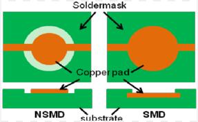
Solder mask defined pads (SMD) are formed by coating solder pads on some copper foils, while unshielded copper foils form solder pads. The opening of the solder mask is smaller than that of the copper solder pad. Solder-resistant pads are suitable for fine-pitch components and are typically used in conjunction with BGA.

The difference between solder mask defined pad (SMD) and non-solder mask defined pad (NSMD)
Solder mask defined pad and non-solder mask defined pad refers to the exposed pad layout design of copper foil solder pads or pads seen on circuit boards.
Solder mask defined pad and non-solder mask defined pas are two ways of exposing solder pads in PCB design, which have emerged in the industry trend of miniaturization of electronic component solder joints or solder balls. This design method is particularly important in ensuring the soldering quality of miniaturized devices, especially miniaturized BGA devices.
1. Definition
1) Solder mask defined pad
Solder Mask Defined Pad Design is a design that uses green oil to cover a large area of copper foil, and then exposes the copper foil at the opening of the green paint (which is not covered by the green paint) to form a solder pad.
Solder mask defined pad, the opening of the resistance layer is smaller than that of the metal pad welding process, which reduces the possibility of the welding plate falling off during welding or welding. However, the disadvantage of this method is that it reduces the copper surface area that can be used for solder joint connection and reduces the space between adjacent solder pads, which limits the wire thickness between solder pads and may affect the use of through holes
2) Non-solder mask defined pad
Non-solder mask defined pad designs the copper foil to be smaller than the opening of the solder mask, and the size of the designed solder pad depends on the size of the copper foil.
In the non-solder mask defined pad welding process, the opening of the resistance layer is larger than the opening of the welding plate, providing a larger surface area for the connection of solder joints. Additionally, the gap between solder pads is larger, allowing for wider line width and more through-hole flexibility. However, non-solder mask pads are more prone to detachment during welding and disassembly processes. Nevertheless, non-solder mask defined pad still has better welding performance and is suitable for solder joint sealing gaskets.
2. Characteristics
The solder mask defined pad and non-solder mask defined pad designs each have their advantages and disadvantages, and they also have their characteristics in terms of solder strength and bonding strength between pads and PCBs
1) The actual copper foil size of SMD solder pads is relatively larger than that of NSMD, and the solder pads are also covered and pressed with solder mask oil around them. Therefore, the bonding strength between the solder pads and FR4 is relatively good. During maintenance or rework, the solder pads are not easily detached due to repeated heating.
2) The solder pad of NSMD is made of independent copper foil. During soldering, in addition to the front side of the copper foil, even the vertical sides around the copper foil can receive tin. In comparison, NSMD has a relatively large tin-eating area, so the soldering strength is relatively good.
The actual area of copper foil in NSMD is relatively small, and layout engineers find it easier to route wire traces because the solder pad size is relatively small, and traces can easily pass between BGA solder pads.
In the solder mask defined pad type, the solder mask is smaller than the metal ball pad. In the non-solder mask defined pad type, the solder mask is larger than the metal ball pad. Choose the solder mask defined pad type to minimize issues that may arise during surface mount assembly.
The correct PCB pad design is crucial for effectively soldering components onto the circuit board. For bare pad assembly, there are two common soldering methods: solder mask defined pad and non-solder mask defined pad, each with its characteristics and advantages.