Friends working in the SMT industry know that many reasons for SMT defects are caused by solder paste printing. In order to better control the quality of printed solder paste, SPI has emerged in the SMT industry. SPI stands for Solder Paste Inspection. The widespread use of SPI in SMT contract manufacturing is mainly due to the current development of the electronic manufacturing industry. So what is the role of SPI in SMT contract manufacturing? Next, iPCB will explain to you, hoping to bring you some help!
1. The working principle of SPI utilizes the laser projection principle to project high-precision red laser (with an accuracy of up to 15 microns) onto the surface of printed solder paste, and uses a high-resolution digital camera to separate the laser contour. Based on the horizontal fluctuation of the contour, the thickness change of the solder paste can be calculated and the thickness distribution map of the solder paste can be drawn, which can monitor the printing quality of the solder paste and reduce defects.
2. SPI is usually placed after the SMT solder paste printing machine. After the PCB solder paste is printed, it is transmitted to the SPI through the track for inspection. Can this improve the SMT yield? The answer is yes. More importantly, how to use SPI to screen out PCB boards with poor printing solder paste, and then track why there are defects in the printing solder paste, in order to solve the fundamental problem.
3. Due to the current precision and miniaturization of electronic products, many SMT manufactured electronic components have high precision, so the quality requirements for PCB surface printing solder paste during component mounting are very high. If the quality of solder paste printing can be detected before SMT, it will definitely be more effective than detecting it after SMT reflow bonding, because poor PCBA boards behind the furnace require the use of Luoyang Iron or more complex tools for repair during the repair process, and a slight lack of attention may damage the PCBA. So SMT foundries with SPI detection equipment can avoid the occurrence of these problems.
")
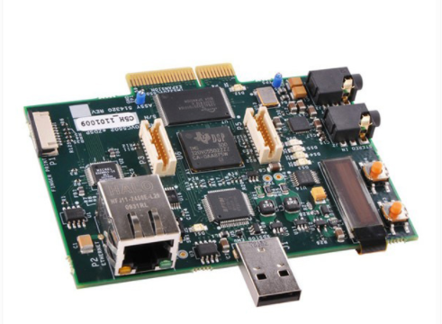
Solder Paste Inspection (SPI)
4. The content of SIP testing includes: solder paste printing quantity, solder paste printing thickness, solder paste printing area, solder paste printing flatness, whether solder paste printing is offset, whether solder paste printing is pointed, and whether solder paste printing is connected.
SPI is a means of quality control in the SMT contract manufacturing process, which can effectively improve product quality and reduce manufacturing costs if used well. If SPI is just a decoration in the SMT workshop, it will only affect production efficiency. If an SPI alarm occurs, it is necessary to investigate the quality of PCB printing solder paste and control the defect rate to the minimum. SPI in SMT contract manufacturing is not only to prevent the quality of solder paste printing, but also to control and prevent maintenance costs in the later stage, which helps to improve production capacity and increase profits.
With the precision of electronic manufacturing products, the quality of printed solder paste has become increasingly important. SPI can effectively ensure good solder paste printing quality and significantly reduce potential quality risks.