With the printed circuit boards of modern wireless communication systems, mobile communication, radar, satellite communication and other communication systems have higher requirements on the switching speed, power capacity, integration, etc. The VXI bus module of the special requirements of the party is of great significance. We will use the idea of virtual instrument to realize the hardware circuit in the form of software. The RF switch designed below can be directly controlled by the computer and can be easily connected with the VXI bus test system. Integrating and maximizing the application of computer and microelectronics technology in today's testing field has broad prospects for development.

1. Design and implementation of VXI bus interface circuit
VXIbus is an extension of VMEbus in the field of instrumentation and is a computer-operated modular automatic instrumentation system. It relies on effective standardization and adopts a modular approach to realize serialization, generalization, and the interchangeability and interoperability of VXIbus instruments. Its open architecture and Plug&Play method fully meet the requirements of information products. It has the advantages of high-speed data transmission, compact structure, flexible configuration, good electromagnetic compatibility, etc., so the system is very convenient to set up and use, and its application is more and more extensive, and it has gradually become a high-performance test system integrated bus.
VXI bus is a completely open, modular instrument backplane bus specification suitable for various instrument manufacturers. VXI bus devices are mainly divided into: register-based devices, message-based devices and memory-based devices. The current proportion of register-based devices in applications (about 70%). The VXIbus register-based interface circuit mainly includes four parts: bus buffer drive, addressing and decoding circuit, data transmission response state machine, configuration and operation register group. In the four parts, except the bus buffer driver is realized by 74ALS245 chip, the rest are realized by FPGA. Adopt a piece of FLEX10K chip EPF10K10QC208-3 and a piece of EPROM chip EPC1441P8, use the corresponding software MAX+PLUS2 to design and implement.
1.1 Bus buffer driver
This part completes the buffer receiving or driving of the data lines, address lines and control lines in the VXI backplane bus to meet the requirements of the VXI normative signal. For A16/D16 devices, as long as the buffer drive of the backplane data bus D00 ~ D15 is realized. According to the requirements of the VXI bus specification, this part is implemented with two 74LS245s, and is gated with DBEN* (generated by the data transmission response state machine).
1.2 Addressing and Decoding Circuits
The addressing lines include address lines A01-A31, data strobe lines DS0* and DS1*, and long word lines LWORD*. The control lines include address strobe lines AS* and read/write signal lines WRITE*. The design of this circuit adopts the schematic design method of MAX+PLUS II. Using the existing components in the component library to design, two pieces of 74688 and one piece of 74138 are used. The function module decodes the address lines A15-A01 and the address modification lines AM5-AM0. When the device is addressed, it receives the address information on the address line and the address modification line, and compares it with the logical address LA7~LA0 set by the hardware address switch on the module. If the logical value on AM5~AM0 is 29H or 2DH (Because it is an A16/D16 device), when the address lines A15 and A14 are both 1, and the logical value on A13-A06 is equal to the logical address of the module, the device is addressed and strobe (CADDR* is true). Then the result is sent to the lower decoding control, and the register of the module in the 16-bit address space is selected by decoding the addresses A01-A05.
1.3 Data transmission response state machine
Data transmission bus is a group of high-speed asynchronous parallel data transmission bus, which is the main component of VMEbus system information exchange. The signal lines of the data transmission bus can be divided into three groups: addressing lines, data lines, and control lines. The design of this part adopts the text input design method of MAX+PLUS2. Since the timing of DTACK* is more complicated, AHDL language is used to design and realize through state machine. This function module configures the control signals in the VXI backplane bus, and provides timing and control signals for the standard data transmission cycle (generating the data transmission enable signal DBEN*, the bus response signal DTACK* required for data transmission, etc.). During data transmission, the system controller first addresses the module, and sets the corresponding address strobe lines AS*, data strobe lines DS0*, DS1*, and WRITE* signal lines that control the direction of data transmission to valid level. When the module detects that the address matches and each control line is valid, it drives DTACK* to a low level to confirm to the bus controller that the data has been placed on the data bus (read cycle) or that data has been successfully received (write cycle). ).
1.4 Configuration Register
Each VXI bus device has a set of "configuration registers", and the system master controller obtains some basic configuration information of the VXI bus device by reading the contents of these registers, such as device type, model, manufacturer, address space (A16, A24, A32) and the required storage space, etc. The basic configuration registers of VXI bus devices are: identification register, device type register, status register, and control register. The design of this part of the circuit adopts the schematic diagram design method of MAX+PLUS II, and uses the 74541 chip, the function module created by it. The ID, DT, and ST registers are all read-only registers, and the control register is a write-only register. In this design, the VXI bus is mainly used to control the on-off of these switches. Therefore, as long as data is written to the channel register, the on-off or off-state of the relay switch can be controlled. Querying the relay state is also read from the channel register. data. According to the design requirements of the module, appropriate content is written in each corresponding data bit, so that the radio frequency switch of the functional module can be effectively controlled.
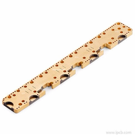
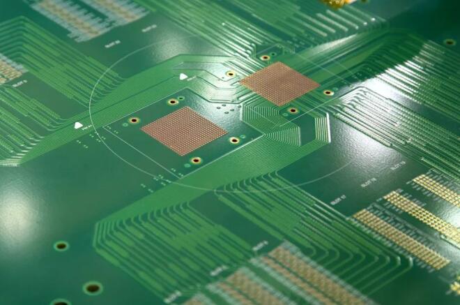
2. Design of module functional circuit PCB board
Each VXI bus device has a set of "configuration registers", and the system master controller obtains some basic configuration information of the VXI bus device by reading the contents of these registers, such as device type, model, manufacturer, address space (A16, A24, A32) and the required storage space, etc. The frequency range of RF circuits is about 10kHz to 300GHz. As the frequency increases, radio frequency circuits exhibit some characteristics that differ from low frequency circuits and DC circuits. Therefore, when designing the PCB board of the RF circuit, it is necessary to pay special attention to the influence of the RF signal on the PCB board. This RF switch circuit is controlled by the VXI bus. In order to reduce interference in the design, a cable is used to connect the bus interface circuit and the RF switch function circuit. The following mainly introduces the design of the PCB board of the RF switch function circuit.
2.1 Layout of components
Electromagnetic compatibility (EMC) refers to the ability of an electronic system to function
normally in a specified electromagnetic environment as designed. For RF circuit PCB design, electromagnetic compatibility requires that each circuit module does not generate electromagnetic radiation as much as possible, and has a certain ability to resist electromagnetic interference. The layout of components directly affects the interference and anti-interference ability of the circuit itself. It also directly affects the performance of the designed circuit.
The general principle of layout: components should be arranged in the same direction as possible, and the phenomenon of poor soldering can be reduced or even avoided by selecting the direction in which the PCB enters the tin melting system; the spacing between components must be at least 0.5mm to meet the tin melting requirements of components, If the space of the PCB board allows, the spacing of the components should be as wide as possible. The reasonable layout of components is also a prerequisite for reasonable wiring, so it should be considered comprehensively. In this design, the relay is the channel used to convert the RF signal, so the relay should be placed as close to the signal input and output as possible, so as to shorten the length of the RF signal line as much as possible, and make a reasonable wiring for the next step. consider. In addition, the RF switch circuit is controlled by the VXI bus, and the influence of the RF signal on the VXI bus control signal is also a problem that must be considered during layout.
2.2 Wiring
After the layout of the components is basically completed, the wiring should be started. The basic principle of wiring is: when the assembly density permits, try to choose a low-density wiring design, and the signal traces should be as thick as possible, which is conducive to impedance matching. For the RF circuit, the unreasonable design of the direction, width and line spacing of the signal lines may cause cross-interference between the signal transmission lines; in addition, the system power supply itself also has noise interference, so it must be comprehensively considered when designing the RF circuit PCB. Reasonable wiring. When wiring, all traces should be kept away from the frame of the PCB board (about 2mm), so as to avoid the possibility of disconnection or potential disconnection during the production of the PCB board. The power line should be as wide as possible to reduce the loop resistance. At the same time, the direction of the power line and the ground line should be consistent with the direction of data transmission to improve the anti-interference ability. The signal lines should be as short as possible, and the number of vias should be minimized; the connection between components should be as short as possible to reduce distribution parameters and mutual electromagnetic interference; for incompatible signal lines, they should be kept away from each other as far as possible., and try to avoid parallel wiring, and the signal lines on the front and back sides should be perpendicular to each other: when wiring, a 135-degree angle should be used where a corner is required, and a right angle should be avoided. In the above design, the PCB board adopts a four-layer board. In order to reduce the influence of the radio frequency signal on the VXI bus control signal, the two signal traces are placed in the middle two layers, and the radio frequency signal line is shielded with ground vias.
2.3 Power and ground wires
The wiring in the RF circuit PCB design needs special emphasis on the correct wiring of the power lin
e and the ground line. Reasonable selection of power supply and grounding method is an important guarantee for the reliable operation of the instrument. Quite a lot of interference sources on the PCB board of the RF circuit are generated by the power supply and the ground wire, and the noise interference caused by the ground wire. According to the size of the PCB board current, the power lines and ground lines should be designed as thick and short as possible to reduce the loop resistance. At the same time, the direction of the power line and the ground line is consistent with the direction of data transmission, which helps to enhance the anti-noise capability. When conditions permit, try to use multi-layer boards. The noise of the four-layer board is 20dB lower than that of the double-layer board, and the noise of the six-layer board is 10dB lower than that of the four-layer board. In the four-layer PCB board designed in this paper, the top and bottom layers are both designed as ground layers. In this way, no matter which layer of the middle layer is the power layer, the physical relationship between the power layer and the ground layer is close to each other, forming a large decoupling capacitor and reducing the interference caused by the ground wire. The ground layer uses a large area of copper. Large-scale copper laying mainly has the following functions:
(1) EMC. For a large area of ground or power supply copper, it will play a shielding role.
(2) PCB process requirements. Generally, in order to ensure the electroplating effect, or the lamination is not deformed, copper is applied to the PCB layer with less wiring.
(3) Signal integrity requirements, give high-frequency digital signals a complete return path, and reduce the wiring of the DC network.
(4) Heat dissipation, special device installation requires copper plating, etc.
3. Conclusion
VXI bus system is a modular instrument bus system that is completely open in the world and is suitable for multi-manufacturers. It is the current instrument bus system in the world. The above mainly introduces the development of the RF switch module based on VXI bus. The design of the bus interface and the PCB design of the functional circuit part of the RF switch module are introduced. The RF switch is controlled by the VXI bus, which increases the flexibility of switch operation and is easy to use on PCB board.