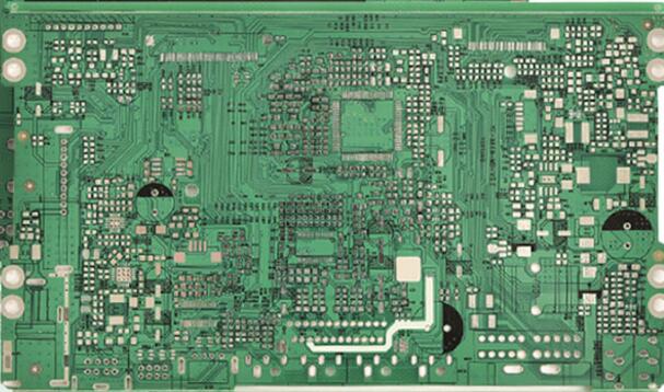
A solder pad is a metal contact point on a PCB used for soldering components, also known as a soldering pad. The solder pad is formed through a copper coating process, usually on both the surface and inner layer of the PCB.

Types of solder pads
According to different uses and manufacturing processes, solder pads can be divided into the following types:
1. Pin pad: Pin pad refers to the metal contact point where pin components are welded on a PCB. Pin pads are usually composed of circular or elliptical metal rings, and pins can be directly inserted into the metal ring for welding.
2. Surface mount pads: Surface mount pads refer to the metal contact points of electronic components welded through SMT on the surface of a PCB. Surface mount pads are usually flat metal pads used to connect the solder pins of SMT components.
3. Through-hole pad: A through-hole pad refers to the metal contact points on the surface and inner layer of a PCB, usually used for welding pin components or connecting inner circuits. A through-hole solder pad consists of a metal ring and a conductive hole.
The function of special pads on PCBs
1. Plum-shaped solder pad
Fixing holes require non-metalization, plum blossom holes, and can always maintain screw grounding regardless of stress changes. Fixed installation holes are usually used as plum blossom pads for GND networks of installation holes, which in some cases serve as shielding for the PCB casing.
2. Cross-pattern solder pad
The cross-shaped solder pad is mainly used to reduce the heat emitted by the solder pad during the welding process, avoiding PCB peeling or solder failure.
3. Teardrop solder pad
Teardrops refer to the excessive connection between solder pads and wires or between wires and holes. Setting tear drops can effectively prevent wire disconnection from holes solder pads or wire contact points, and can also make the PCB circuit board look more beautiful.
The difference between pads and vias
1) Concepts
A solder pad refers to a reserved position on a PCB for soldering chips or components. On a PCB, the pins of the components are connected to the solder pads through welding, thereby achieving electrical and physical connections between the components and the circuit board. So, solder pads are required for each layer on the PCB.
Through holes refer to small holes on the surface of a PCB that are electrically connected to another layer (double-sided board) or multi-layer board (multi-layer board). Through vias, connections at different levels can communicate with each other, making PCB wiring more flexible to a certain extent.
2) Function
Solder pads connect components to achieve physical and electrical connections between components and circuit boards.
Through holes, different layers achieve connectivity between various parts of the circuit, thus achieving normal operation of the circuit.
3) Shape and Design
The solder pads are generally circular or square, and their size and shape depend on the requirements of the components. In terms of pad design, it is necessary to ensure that the size of the pad can meet the welding requirements of the components on top, while also considering the spacing between components to avoid problems such as short circuits due to being too close.
The via is achieved through electrolytic copper, and the position and diameter of the via need to be considered in the design. For multi-layer PCBs, it is also necessary to consider the number and distribution of vias to ensure electrical performance and signal transmission stability.
4) Processing method
Solder pads are generally made by chemical copper plating, and then the outer layer of the pad is electroplated to ensure its corrosion resistance and conductivity.
Through holes are made by drilling holes on the board surface and then chemically plating copper.
The types of PCB solder pads are different, but their functions are consistent. One is to achieve the electrical connection of electronic components in the circuit; The second is to enable external electronic components to be better connected to the PCB circuit board, playing a role in preventing detachment.