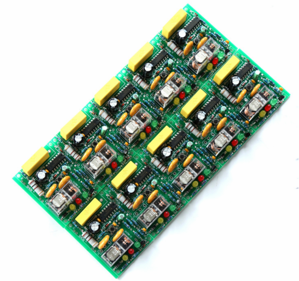
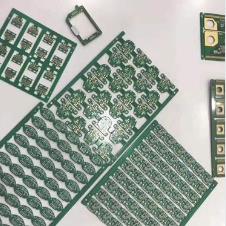
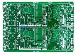
what is solder resist?Solder resist, also known as a protective agent or overlay, is a coating material used to protect copper alignments and via holes on PCBs from the environment. It usually consists of components such as resins, fillers, and additives, and is applied to the surface of the PCB by means such as screen printing or spraying. Soldermask serves to provide insulation, prevent short circuits, enhance the solderability of the via holes, and protect the wiring from mechanical damage and chemical corrosion.
The commonly used PCB solder mask types are solder,seam solder, and butt solder, but the problems that often occur during the solder mask process include substrate bumps, false copper exposure, uneven solder mask, internal circuit breakage, etc.In the production process, Zhuolu Electronics will make sure to pay attention to the operation points of each step when handling the solder mask, and ensure that it provides customers with high-quality PCBs.
First of all, why do we do solder mask. The purpose of solder mask mainly includes the following points:

1. Leave the through holes and their pads on the PCB to be soldered to cover all the circuits and copper surfaces to prevent short circuits caused by PCB wave soldering and save the amount of solder.
2. Prevent moisture and various electrolytes from oxidizing the circuit and endangering electrical performance, and prevent external mechanical damage to maintain good insulation on the board.
3. As the board becomes thinner and lighter as the board is produced, the line width becomes thinner and thinner, so the insulation problem between the conductors has become increasingly prominent, and the importance of the insulation performance of the solder resist is also increased.
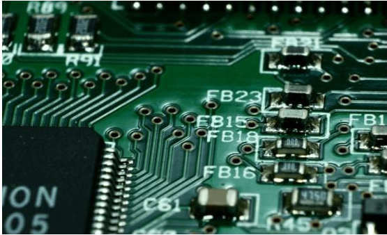
Secondly, everyone in the PCB industry understands that: the solder mask refers to the part of the board that needs to be evenly coated with green paint, but in fact the green solder mask uses a negative output, so the shape of the green solder mask is mapped to the board After the application, the solder mask was not painted with green oil, but the copper skin was exposed. In the production process, usually in order to increase the thickness of the copper skin, the method of scribing on the solder mask will be used to remove the green oil. The solder mask plays an important role in controlling the soldering defects during the reflow soldering process. The PCB designer should minimize the spacing or air gap around the pad during the design, or it can be handed over to our engineers.
For the solder mask process, there should be too many changes for the time being, but process innovation is everywhere. The future development of PCB production and processing will encounter various challenges, no matter what kind of challenge, as long as the PCB factory maintains I believe that the future development will not be bad when I update my own technology. Materials, equipment, and PCB manufacturers will face challenges and even great pressure to survive. Domestic PCB manufacturers are at a relative disadvantage in the fields of HDI, automotive boards, and IC substrates, and require more investment. It is necessary for material vendors, equipment vendors, and manufacturers to reach closer cooperation beyond the pure interest relationship. Of course, different companies need to position their products differently. They should not all develop into HDI, automotive electronics PCB boards, and IC packaging substrates. For companies, it is not the harder the better, nor the more sophisticated, the better. The one that suits you is the best. OK.