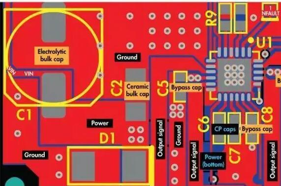
PCB routing bypass capacitor refers to the addition of capacitors next to circuit routing in PCB design to reduce noise and improve signal integrity and stability. In high-frequency circuit design, bypass capacitance is a commonly used solution, which can effectively eliminate noise interference in the circuit and improve the quality of signal transmission.

A capacitor is an abbreviation for a capacitor, consisting of two conductors that are close to each other, with a layer of non-conductive insulating medium sandwiched between them. When a voltage is applied between the two plates of a capacitor, the capacitor will store charge.
Capacitors connected in parallel with the load in the circuit can resist voltage changes caused by current changes, making the working voltage of the load more stable.
The use of capacitors, resistors, and inductors in the signal transmission circuit can form various filters to purify the signal.
How to place capacitors in PCB design
Capacitors play an important role in high-speed PCB design and are usually the most commonly used device on PCBs. In PCB, capacitors are usually divided into filtering capacitors, decoupling capacitors, energy storage capacitors, etc.
1. Power output capacitor, filtering capacitor
We usually refer to the capacitors in the input and output circuits of the power module as filtering capacitors. Simply understood, it is a capacitor that ensures stable input and output power supply. The principle of placing filter capacitors in the power module is "first large and then small".
When designing the power supply, attention should be paid to the wiring and copper sheet being wide enough, and the number of through holes being sufficient to ensure that the current capacity meets the requirements. Evaluate by combining the width and number of vias with the current magnitude.
2 decoupling capacitors
The power pins of high-speed ICs require sufficient decoupling capacitors, and it is best to ensure that each pin has one. In actual design, if there is no space to place decoupling capacitors, they can be removed as appropriate.
The capacitance value of the decoupling capacitor of the IC power supply pin is usually relatively small, such as 0.1 μ F. 0.01 μ F, etc; The corresponding packaging is also relatively small, such as 0402 packaging, 0603 packaging, etc. When placing decoupling capacitors, the following points should be noted.
1) Place as close to the power pins as possible, otherwise decoupling may not be effective. In theory, capacitors have a certain range of decoupling radius, so the principle of proximity should be strictly followed.
2) The lead from the decoupling capacitor to the power pin should be as short as possible, and the lead should be thickened, usually with a line width of 8-15 mils (1mil=0.0254mm). The purpose of bolding is to reduce the lead inductance and ensure power performance.
3) After the power and ground pins of the decoupling capacitor are led out from the solder pad, holes are drilled nearby and connected to the power and ground plane. The lead wire should also be thickened, and the through-hole should be as large as possible. If a hole with a diameter of 10mil can be used, an 8mil hole is not needed.
4) Ensure that the decoupling loop is as small as possible. The common BGA packaging typically has decoupling capacitors placed underneath the BGA, i.e. on the back. Due to the high pin density of BGA packaging, decoupling capacitors are generally not placed in large quantities, but they should be placed as many as possible.
3. Energy storage capacitor
The function of energy storage capacitors is to ensure that the IC can provide electrical energy in the shortest possible time when using electricity. The capacitance value of energy storage capacitors is generally relatively large, and the corresponding packaging is also relatively large. In a PCB, the energy storage capacitor can be located further away from the device, but it cannot be too far either.
The principles of capacitor fan holes and fan wires are as follows.
1) Try to make the lead as short and bold as possible to reduce parasitic inductance.
2) For energy storage capacitors or devices with high overcurrent, it is advisable to drill as many holes as possible.
3) Of course, the best electrical performance fan hole is the hole in the disc. Actual needs to be comprehensively considered.
A capacitor, also known as "capacitance", refers to the amount of free charge stored under a given potential difference, and is one of the common and important passive devices in circuit design. Capacitors often play an important role in high-speed circuits. From the perspective of circuit properties, passive devices have two basic characteristics: (1) they either consume electrical energy themselves or convert electrical energy into other forms of energy. (2) You only need to input a signal and can work normally without the need for an external power source. There are generally many types of functions and uses for capacitors. For example, the role in bypass, decoupling, filtering, and energy storage; Complete oscillation, synchronization, and time constant.