The via itself has a parasitic capacitance to the ground. If it is known that the diameter of the isolation hole on the ground layer of the via is D2, the diameter of the via pad is D1, the thickness of the PCB circuit board is T, and the substrate dielectric is Changshu Is ε, then the parasitic capacitance of the via is approximately as follows:
C=1.41εTD1/(D2-D1)
The main effect of the parasitic capacitance of the via hole on the circuit is to extend the rise time of the signal and reduce the speed of the circuit. For example, for a PCB with a thickness of 50Mil, if the inner diameter is 10Mil, the pad diameter is 20Mil For the via, the distance between the pad and the ground copper area is 30Mil, then we can use the approximate value of the above formula to calculate the parasitic capacitance of the via:

C=1.41x4.4x0.05x0.02/(0.032-0.020)=0.517pF, the change in rise time caused by this part of the capacitance is:
T10-90=2.2C(Z0/2)=2.2x0.517x(55/2)=31.28ps. It can be seen from these values that although the effect of the rise delay caused by the parasitic capacitance of a single via is not obvious, if the via is used multiple times in the trace to switch between layers, the designer should still consider carefully.
One, the parasitic inductance of the via
Similarly, there are parasitic capacitances in vias and parasitic inductances. In the design of high-speed digital circuits, the damage caused by the parasitic inductances of vias is often greater than the impact of parasitic capacitance. Its parasitic series inductance will weaken the contribution of the bypass capacitor and weaken the filtering effect of the entire power system. The following formula can be used to simply calculate the parasitic inductance of a via:
L=5.08h[1n(4h/d)+1] where L refers to the inductance of the via, h is the length of the via, and d is the diameter of the center hole. It can be seen from the formula that the diameter of the via has a small influence on the inductance, and the length of the via has the greatest influence on the inductance. Still using the above example, the inductance of the via can be calculated as:
L-5.08x0.050[1n(4x0.050/0.010)+1]=1.015nH. If the rise time of the signal is 1ns, then its equivalent impedance is: XL=πL/T10-90=3.19Ω. Such impedance can no longer be ignored when high-frequency currents pass. Special attention should be paid to the fact that the bypass capacitor needs to pass through two vias when connecting the power plane and the ground plane, so that the parasitic inductance of the vias will increase exponentially.
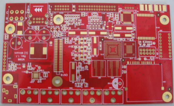
2. Via design in high-speed PCB
Through the above analysis of the parasitic characteristics of vias, we can see that in high-speed PCB design, seemingly simple vias often bring great negative effects to the circuit design. In order to reduce the adverse effects caused by the parasitic effects of the vias, the following can be done in the design:
1. Considering both cost and signal quality, select a reasonable size via size. For example, for the 6-10 layer memory module PCB design, it is better to use 10/20Mil (drilled/pad) vias. For some high-density small-size boards, you can also try to use 8/18Mil. hole. Under current technical conditions, it is difficult to use smaller vias. For power or ground vias, you can consider using a larger size to reduce impedance.
2. The two formulas discussed above can be concluded that the use of a thinner PCB is beneficial to reduce the two parasitic parameters of the via.
3. The signal traces on the PCB board should not be changed as much as possible, that is to say, try not to use unnecessary vias.
4. The power and ground pins should be drilled nearby. The shorter the lead between the via and the pin, the better, because they will increase the inductance. At the same time, the power and ground leads should be as thick as possible to reduce impedance.
5. Place some grounded vias near the vias of the signal layer changeover to provide the nearest loop for the signal. It is even possible to place a large number of more ground vias on the printed circuit board. Of course, the design needs to be flexible. The via model discussed earlier is the case where there are pads on each layer, and sometimes, the pads of some layers can be reduced or even removed. Especially in the case of a very high density of vias, it may lead to the formation of a slot that separates the loop in the copper layer. To solve this problem, in addition to moving the position of the via, you can also consider placing the via on the copper layer. The pad size is reduced.