HDI (High Density Interconnect Transistor) is a high-density interconnection board, circuit board and dense circuit distribution using micro-shielded aperture technology. The crystalline inside the porosity can be connected to the inside of each row. The HDI table is generated by backward methods, and the number of layers is high, and the technical level is very high.
HDI is mainly a layer of trees. HDI uses two or more techniques, using pigs, clothing, direct lasers, etc. When the density of PCBs exceeds 8 laminates, the production cost will be lower than the cost of more traditional pressure solutions.
HDI board is useful for using advanced packaging technology and its wrapper. Optimize HDI signal in terms of radio frequency interference, electromagnetic interference, release and conductivity. Electronic products continue to expand to high density and high precision, which means that after the performance of the machine is improved, the volume of the machine must be reduced.
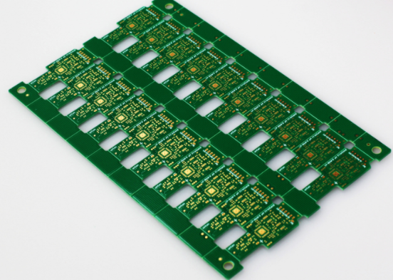
Single-layer PCB board,multi-layer circuit board
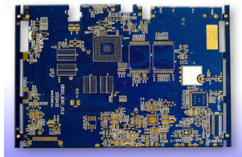
E performance standards and electronic efficiency standards. Currently, electronic products, such as mobile phones, images (photos), notebook computers, automotive electronics, etc. Polychlorinated biphenyls Introduction PCB (PPCE Circle Board) is a printed circuit board and a printed circuit board, an important electronic component, an electronic component holder, and a carrier for electronic components.
He is called "printed matter" This is mainly due to the use of printed boards under the confidentiality of the same kind of printed boards, thus avoiding routing errors. Artificial, from Hand, Hand, Self-Power, equipment quality, and improved methods.

Do all PCB panels refer to the name of HDI?
HDI card, namely high-density interconnection board, and the other two braille chips are HDI board, minister level, third level, scale and other levels, such as iPhone 6. Simple burying does not necessarily mean that HDI PCB is relatively simple, and the process and process are well controlled.
This is a position problem, it is a problem of pants and copper. The second order is designed in a different way, and it is the identity of the place of purchase connected to the middle layer.
is connected to two HDI levels from adjacent layers.
Double layer circuit board
The second question is that these two orders overlap each other. The second order is carried out through the super position. The treatment is similar to the two steps, but there are many treatment factors that must be simple, which means I’m sorry.
The third party opens directly to the third layer (or second layer).
This is the third level analogy. HDI and PCB common PCB. The normal blades of the PCB plate are mainly F-4, which is used for epoxy resin and electronic glass.
On the outside, copper foil is generally used in traditional HDI, because laser drilling is not in the form of glass. There is no difference between ordinary materials.