PCB stack structure design recommendations
The PCB stacking method is recommended to be the Foil stacking method
2. Minimize the use of PP sheets and CORE models and types in the same stack (each layer of medium does not exceed 3 PP stacks)
3. The thickness of the PP medium between the two layers should not exceed 21MIL (thick PP medium is difficult to process, generally adding a core board will increase the actual number of layers and increase the processing cost)
4. The outer layer (Bottom layer) of the PCB is generally 0.5OZ thick copper foil, and the inner layer is generally 1OZ thick copper foil.
Note: The copper foil thickness is generally determined according to the size of the current and the thickness of the trace. For example, the power board generally uses 2-3OZ copper foil, and the ordinary signal board generally chooses 1OZ copper foil. If the trace is thinner, 1/3QZ copper may be used. Foil to improve the yield; at the same time, avoid using core boards with inconsistent copper foil thickness on both sides of the inner layer.

5. The distribution of the PCB wiring layer and the plane layer must be symmetrical from the center line of the PCB stack (including the number of layers, the distance from the center line, the copper thickness of the wiring layer and other parameters)
Note: The PCB stacking method needs to adopt a symmetrical design. The symmetrical design refers to the thickness of the insulation layer, the type of prepreg, the thickness of the copper foil, and the pattern distribution type (large copper foil layer, circuit layer) as symmetrical to the center line of the PCB as possible.
6. The design of line width and medium thickness needs to leave sufficient margin to avoid design problems such as SI caused by insufficient margin
The stack of PCB is composed of power layer, ground layer and signal layer. As the name suggests, the signal layer is the wiring layer of the signal line. The power layer and the ground layer are sometimes collectively referred to as the plane layer.
The stack of PCB is composed of power layer, ground layer and signal layer. As the name suggests, the signal layer is the wiring layer of the signal line. The power layer and the ground layer are sometimes collectively referred to as the plane layer.
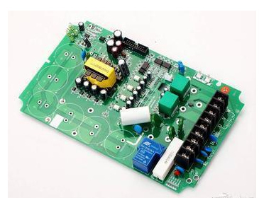
After the customized PCB circuit board is completed, the next step is SMT placement. According to the BOM list provided by the customer, the purchased components are subjected to SMT loading, and then through the entire process of DIP plug-in (Note: SMT and DIP are both in PCB The difference in the way of integrating parts on the board is that SMT does not need to drill holes on the PCB board, just insert the PIN pins into the holes that have been drilled.) The production line for processing components is referred to as "SMT patch line". For surface mount technology, the use of mounters to mount some tiny parts on the PCB board (process: positioning, printing solder paste, mounter mounting, reflow oven and manufacturing inspection) DIP can also be called " "Plug-in", that is, inserting parts on the PCB board. This is the integration of parts in the form of plug-ins when some parts are larger in size and are not suitable for placement technology.
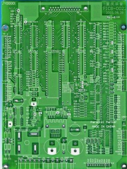
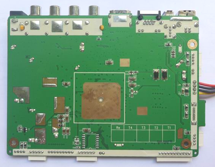
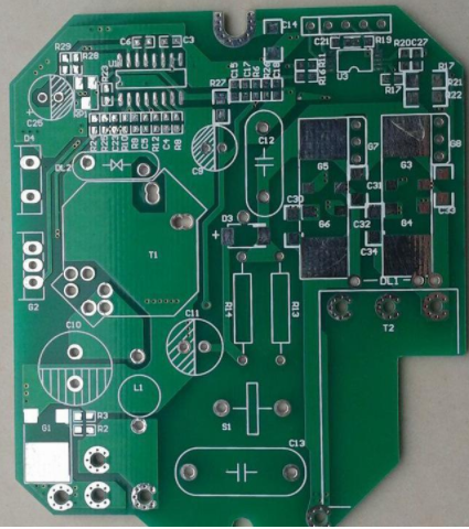
Through the above introduction, I believe that everyone has a certain understanding of PCBA. In layman's terms,SMT patch refers to a processing process. PCBA can also be understood as a finished circuit board. Device IC), and PCB can be understood as: PCB bare board (also called light board, there is nothing on it except for lines)