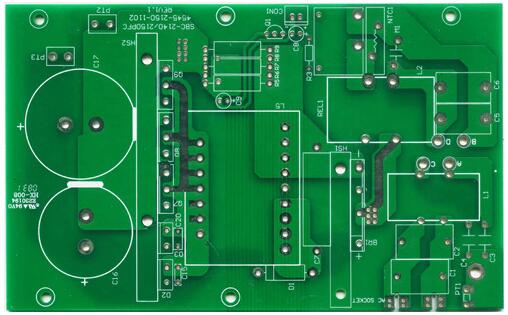
In the PCB factory production, is it possible to allow wire patching? What are the norms that can be followed? For example, how long and how wide the line can not be filled? How many refills can be allowed on a board? What characteristics will be affected by the repaired circuit board?
"Fixing" is a traditional circuit board repair method, which is mainly used to repair the inner layer. In the outer layer, it is relatively rare that manufacturers are willing to allow repairs to occur. When the working frequency of information products is not high, it can still be used to rescue the boards with open circuit defects. Most manufacturers will define the working size of the board in production, and it is more common that each board allows one line to be repaired.
However, most of the current products have a high operating frequency, many have reached 1GHz or higher transmission speed (High Speed), any signal line defects (nick, protruding Protrusion, pin hole, pin hole, pit Pit, depression, indentation) Dish Down), etc., may cause degradation of "Signal Integrity", slower transmission speed and unstable characteristic impedance. Especially for high frequency (High Frequency) microwave communication products, there are strict requirements for the thickness of the line and the residual foot of the line. Of course, these products cannot be used to make up the line at all.
For products that are still allowed to be repaired, the industry can start construction according to IPC-R-700 or the new document IPC-7721. As for the operating methods and acceptance rules, they are not included in the formal IPC documented specifications, and the coordination of specifications and quality must be discussed by both parties.
The thickness of the PCB board cannot be edged when the thickness is in mm
In which process does the PCB generally need to be edging, is it pressing or drilling? What is the thickness of the board when it is not possible to grind? Are there points? Which equipment vendors provide edging equipment?

The main purpose of edging is to reduce the trouble caused by swarf in the cutting process. Therefore, it is possible to use this process for any process that produces lint on the edge of the circuit board. Perhaps it would be more appropriate to change the edging to trimming, because most manufacturers currently use tools for trimming rather than grinding.
Trimming procedures are implemented in many places in the circuit board manufacturing process, such as: after material distribution, trimming after pressing, trimming after electroplating, trimming after finished product cutting, gold finger trimming, etc. The main purposes of these edging actions are mostly concentrated in two aspects. The first is to avoid scratching the operator, machinery and tools or negatives used. As for the final product, it is beautiful and convenient to assemble and operate. The second is for possible pollution caused by the dander, because the burrs are easy to fall off and the debris is not easy to clean. If they fall into the tank of the production process, problems such as roughness and pollution can easily occur. Of course, for products with wider quality requirements, these treatments may also be discarded.
The importance of edging is extremely important in exposure, electroplating processes or other processes that are highly sensitive to particles. If you skip this procedure and work directly, then quality problems will easily occur. As for whether to use trimming, in addition to quality considerations, cutting process capability is also one of the issues. Because there is no proper mechanism to repair thinner circuit boards, most manufacturers will abandon trimming without proper equipment. But also because the plate thickness is thin, the degree of burrs is not too high and the impact is limited. Most of the manufacturers work hard to improve the cutting of thin plates and reduce the burrs to avoid edge grinding.
How thin the circuit board does not need to be edged? There is no standard answer, but it is said that for thin plates below 16mil, edging becomes difficult gradually. At present, there are equipments that can perform circuit board trimming operations, and it is also equipped with the corner rounding function. The design of this type of equipment is the same as the concept of traditional edge planing with V-shaped cutters, except that the V-shaped cutter is designed as a high-speed rotating cutter to remove board edge swarf during the travel of the circuit board.
For thinner materials, this type of equipment needs to cut a little material width to perform, so it always feels unsatisfactory for PCB manufacturers who are very concerned about material utilization. However, from practical experience, the processed materials are indeed helpful for quality improvement. The above is for reference only.